Products that need semiconductor materials to function include electronic devices and components, and these materials have specifically seen increased demand due to their use in many of the ‘clean energy’ items we see today, like solar cells, IoT sensors, and self-driving car circuits. The most used semiconductor materials, according to the Institute of Electrical and Electronics Engineers (IEEE), are silicon, germanium, and gallium arsenide.
Because semiconductor materials have specific characteristics related to electrical conductivity, it is crucial that manufacturers have quality control technologies and procedures in place during research, development, and manufacturing, to help ensure the products perform as expected.
Vibrational spectroscopy techniques (including mid- and far-infrared, near-infrared, and Raman) provide powerful options for analyzing and optimizing semiconductor materials. This article will address the role Raman spectroscopy can play in this industry.
About Raman Spectroscopy
Raman spectroscopy is a powerful tool for characterizing semiconductor materials like silicon-based copper, indium, gallium, diselenide solar cells, cadmium, telluride-based organics, and III-Vs. It provides valuable information on:
- chemical compositions,
- polytypes,
- stress and strain,
- concentration of dopants,
- thickness of films,
- type of crystal and orientation,
- crystal quality including defects, uniformity, contaminants, or purity, and
- device temperature.
Raman spectroscopy is particularly effective in measuring the crystallanity of samples. For example, the silicon-silicon bond, a symmetrical covalent bond, is ideal for Raman. This technique is sensitive to small changes in these bonds, making it an excellent tool for such measurements. It can discern different silicon morphologies, distinguishing between crystalline and amorphous forms in the sample.
Beyond qualitative analysis, Raman spectroscopy can also be used for quantitative analysis. A calibration curve can be constructed using samples of known composition, with peak height or peak area used as key indicators. For example, in the case of silicon, the height of the crystalline silicon peak to the amorphous silicon peak can be used to extract information about a larger sample area.
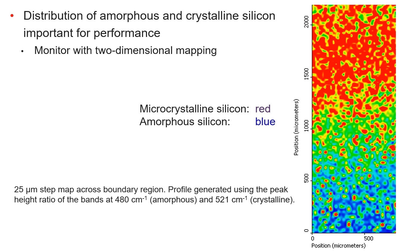
Mapping is a powerful technique and can be done by selecting various points on the sample for analysis. This point-by-point approach is especially useful for analyzing samples where there may be a compositional variance. The spectral data can be depicted as an image, showing the spectra for each location stacked on top of each other, providing a chemical zone or spectral map. Distribution of amorphous and crystalline silicon is important for performance. This can be monitored with two-dimensional mapping.
Raman spectroscopy instruments can also provide the ability to generate a profile based on the spectral feature, the height peak area, and ratios. This feature is demonstrated below using an example of a silicon sample where areas of high signal intensity are shown in red, corresponding to the crystalline peak of silicon, and diffuse blue-green regions corresponding to the amorphous silicon peaks.
Raman spectroscopy is also used to analyze other active materials used in solar applications and the semiconductor industry, such as Silicon Carbide, Cadmium Telluride, and Copper Indium Gallium Diselenide (CIGS).
As you can see, Raman spectroscopy is a powerful and versatile tool for the analysis of semiconductors, offering both qualitative and quantitative data. It is effective, easy to set up, and can provide a wealth of information about the sample being analyzed.
Our Raman spectroscopy expert presents additional information about Raman spectroscopy for semiconductor analysis, and shows specific examples of how to measure silicon crystallinity and map samples in this video.
Additional Resources
- Raman Microscope application notes
- Analytical Solutions for Semiconductor Manufacturing
- Raman Spectroscopy Academy
- Video: Raman Spectroscopy for Semiconductor Analysis
Leave a Reply