History of NAND flash devices
3D NAND flash memory devices have come a long way over the last half decade. Five years ago, 2D planar NAND consisted of billions of memory cells densely packed next to each other to provide higher capacity flash with faster performance. As the ability to pack more cells into sub 1x nanometer planar NAND reached its limits, manufacturers turned to 3D NAND, a groundbreaking technology stacking memory cells on top of each other in multiple layers to achieve higher-capacity, greater reliability, and faster write speeds.
3D NAND flash memory
The first 3D NAND flash memory started shipping in 2013 with 24-layers. The revolutionary process introduced a chemical vapor deposition (CVD) process to stack thin film layers connected with precise holes etched through the entire vertical structure. Through the years, the need to increase capacity to meet data storage demands pushed manufacturers to higher aspect ratios with 3D NAND advancing to 64, 96, 128, 144 and most recently, 176-layers.
As layers of memory cells have been added, increasing performance, storage capacity and energy efficiency, the complexity of the fabrication process has also increased. Precise deposition and etching processes have become more challenging, resulting in longer manufacturing times and buried defects in word lines and control gates. Moreover, errors introduced into the fabrication process — such as non-uniform layer thickness or incomplete, bowed or twisted etched holes — can result in lower yield per wafer and higher costs per terabyte.
3D NAND analysis
Today, many 3D NAND manufacturers send samples to a lab for analysis. Between transit time, waiting for the lab to process the sample and receiving the results, the fab can be delayed for days and even weeks. This leads to longer development cycles, increased manufacturing cost, slower time-to-market, and reduced profits. But what if there was a better way for the fab to more quickly get the data and insights they need to improve and maximize their processes?
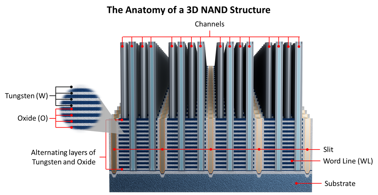
As 3D NAND layer counts increase, it’s increasingly difficult to identify defects in these complex high-aspect ratio structures—slowing development cycles and increasing cost-per-bit.
An inline, easy-to-use system that combines high-resolution, high-contrast imaging with automated delayering and milling would allow busy fabrication customers to obtain unprecedented insights into the entire stack of their high-aspect ratio structures, right within the fab. This would significantly reduce time-to-data, accelerate process and device development, and bring innovative products to market more quickly.
Our new Helios 5 PXL PFIB Wafer DualBeam reduces time-to-data for through-stack metrology of advanced 3D structures from days to hours.

Sean Zumwalt is a Senior Marketing Manager for semiconductors at Thermo Fisher Scientific.
///
Physical and Electrical Failure Analysis of Power Semiconductor Devices
World energy consumption is expected to grow by nearly 50% b...
Read More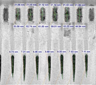
Revolutionizing the way TEM metrology data is collected
As I discussed in my 2024 year-end article, the semiconducto...
Read More
Leave a Reply