For decades, the semiconductor industry has been defined by its ability to innovate. Each time it’s faced new challenges, it’s found innovative ways to overcome these and deliver greater performance to meet computing needs. Today, we’re seeing this innovation continue as the advanced semiconductor packaging industry works to broaden the adoption of chiplets to deliver the next-generation of chip designs and packages.
Where historically integrated circuit (IC) vendors would design a chip that integrated more functions on the same die, for many, scaling planar 2D designs become extremely difficult and costly. This resulted in many pursuing advanced packaging strategies, such as 2.5D-IC, 3D-IC and 3D wafer-level packaging (3D-WLP), that combine chips at different process nodes and chiplets. For these vendors, advanced packaging provides a cost-effective way to enhance semiconductor device performance, develop solutions faster, and design customized solutions for specific applications and markets. While advanced semiconductor packaging technology has great potential, designing and manufacturing it is not without its challenges, as the integration of chips at different process nodes and chiplets is not a simple process.

IC design costs over time, Source: IBS
Advanced semiconductor packaging challenges
For advanced packaging manufacturers, designing a stacked chip-based semiconductor device requires the product architecture, known-good die, die-to-die interconnects and robust manufacturing capabilities. Coupled with increasingly more complex 3D structures, identifying defects buried in the structure can be challenging. Examples of some of the challenges and encountered defects include:
- Die-level defects from metal shorts, particles and silicon cracks
- Wafer thinning and bonding issues related to grinding, wet etching and inter-die connections
- Through silicon via (TSV) formation problems attributable to TSV patterning, etching and filling
- Bump issues from shorts and metal protrusions
- Substrate problems attributed to via cracks, ball grid array (BGA) contamination and solder reflow
When defects such as these occur, the result is often a non-functional semiconductor device or a device that will fail in the future.
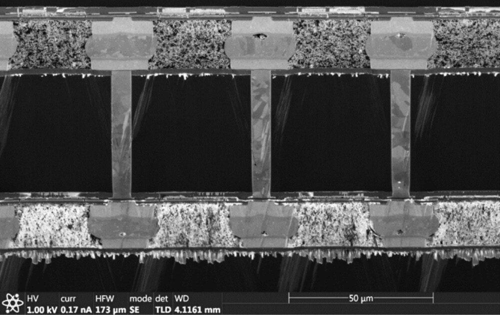
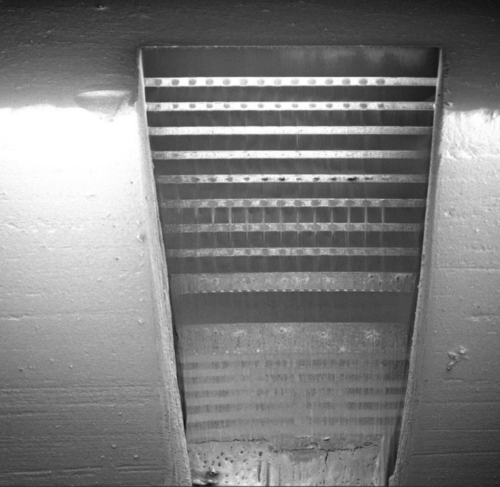
Bumps, bonds and interposer, and chip stacking through TSV exposed by PFA analysis
To address these challenges, there is a need to see inside the device to accurately identify defects potentially impacting scrap costs, yields and performance. This is where a combination of electrical failure analysis (EFA) and physical failure analysis (PFA) solutions can be extremely beneficial in assisting advanced packaging vendors.
Solutions for identifying defects
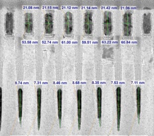
For the user, an EFA solution such as the Thermo Scientific Elite System, provides fast and precise fault localization of defects with amplitude and phase data for x, y and z-dimensions. For root cause analysis, a PFA solution such as the Thermo Scientific Helios 5 PFIB provides Sub-nanometer SEM imaging resolution for visualization of small structures and features.
Together, they provide a complete solution to assist advanced semiconductor packaging manufacturers in delivering the next generation of chip designs.
For more information on this topic, please visit our Advanced Packaging webpage or watch our on-demand SPARK webinar, Unpacking Packaging Challenges.

David Akerson is a Sr. Marketing Manager at Thermo Fisher Scientific
Revolutionizing the way TEM metrology data is collected
As I discussed in my 2024 year-end article, the semiconducto...
Read MoreSemiconductor Nanoprobing Boosts TEM Analysis Success Rates on Advanced Logic Devices
Growing need for semiconductor nanoprobing As the semiconduc...
Read More
Accelerating Semiconductor Device Analysis with the Power of the Helios 5 EXL Wafer DualBeam
Semiconductor fabrication challenges Semiconductor fabricati...
Read MoreFailure analysis of wide bandgap semiconductor devices
Compound semiconductors create analytical challenges Our eve...
Read More
Leave a Reply