Display technology relies on a complex, multi-stage manufacturing process. Along the way, failure analysis of semiconductor devices can be used to improve quality and yield, and the greatest benefits come from applying failure analysis to display backplanes, panels, and modules.
Failure analysis of semiconductor devices: unwanted particles and panel defects
As display resolution increases, failures can be caused by particles that are too small to detect with typical optical microscopy workflows. Also, the increasing complexity of display technology is more likely to bury unwanted particles deep inside the structure, obscuring them from optical view. Figure 1 illustrates the display stack from a mobile device, and the red boxes highlight the areas that are especially susceptible to particle contamination.
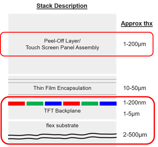
Figure 1: This example display stack highlights the layers that can affect yield, quality and performance.
A high-resolution scanning electron microscope (SEM) can be used to find and resolve backplane particles (Figure 2). Using a SEM along with X-ray energy-dispersive spectroscopy analysis can provide elemental information (e.g., material composition). This helps failure analysts isolate the root causes of unwanted particles and then identify ways to reduce their occurrence.
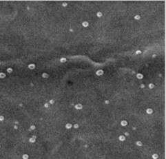
Figure 2. Backplane particles imaged by a Thermo Scientific Apreo 2 SEM.
As more architectural elements are built onto the backplane, unwanted particles can create panel defects that cause dead pixels and other potentially fatal flaws. Within these complex problems, electronic device failure analysis requires a workflow that proceeds from coarse to fine localization of defects.
Accurately isolating faults and finding killer defects is a key challenge. Evolving display technologies demand approaches such as lock-in thermography to detect the temperature variations that lead to device failures. Compared to optical approaches, the Thermo Scientific Elite System is a powerful lock-in thermography tool with an extremely high success rate in the isolation of electrical faults. Specifically, Elite can detect electrical faults in the thin-film transistor backplane, in either the thin-film transistor matrix or the controller area, with precision on the order of a few micrometers.
The next step is to locate defects more precisely by running electrical tests on the thin-film transistor backplane. Here, the challenge is in carefully removing just enough material to expose the underlying circuitry. This has typically been done using chemical etching; however, this approach is not site-specific and can potentially damage the circuit of interest.
Greater precision and repeatability are possible with gas-enhanced etching applied using a Thermo Scientific Helios 5 Plasma Focused Ion Beam (PFIB). The delayering process can open a window of approximately 50 by 50 microns square. Then, it can homogeneously remove material above the circuit, expose the metal, and prepare the surface for electrical testing (Figure 3).

Figure 3. Precise delayering enables accurate probing and informative electrical testing of embedded circuits.
Electrical probing is then used to pinpoint the locations of panel defects. Depending on the size of the features, this could entail micro-probing with optical microscopy or nano-probing using the SEM.
The sample can then be moved to a dual-beam system such as the Thermo Scientific Helios 5 Small DualBeam for cross-sectional “slice and view” visualization and analysis of the region around the defect (Figure 4). For especially small defects that require comprehensive analysis, the Small DualBeam can be used to prepare thin samples for visualization using a transmission electron microscope (TEM), such as the Thermo Scientific Talos F200E.

Figure 4. Locating and analyzing defects deep inside display panels with the Thermo Scientific Helios 5 Small DualBeam.
Milling and imaging multi-layer display modules
In display modules, other parts of the packaging are attached to the panel: the touchscreen assembly, the peel-off layer (Figure 1), and connections to driver ICs and flexible PCBs. Here, electronic device failure analysis depends on methods that accurately locate defects through many types of packaging materials.
Elite excels here, too. As a first step, it can be used to locate faults by identifying hotspots in touch-panel sensors, flexible PCBs, bumping areas, or driver ICs. Next, each defect is accessed and analyzed. Rather than deconstructing the packaged module, the Helios 5 PFIB can be used to mill through different materials for full-stack cross-sectional analysis spanning large areas (Figure 5). For display modules, a PFIB is the most reliable and straightforward way to perform direct and detailed physical failure analysis.

Figure 5. After precise milling with Helios 5 PFIB (left), high-resolution imaging is used to analyze individual layers such as anisotropic conductive adhesives (right).
Improving quality and yield with early failure analysis of semiconductor devices
For failure analysis of semiconductor devices in display modules, panels and backplanes, Thermo Fisher offers solutions that provide accurate fault isolation combined with root-cause analysis. When applied as early as possible, the result is an ability to improve quality and yield in the manufacturing of increasingly complex, high-resolution display panels.
To be continued
This post is the third in our series of four focused on display technology. The second narrowed in on advanced process metrology for examining crucial layers of display technology, and the next will focus on the technology roadmap as it relates to R&D in materials science.

//
Xiaoting Gu is a product marketing manager at Thermo Fisher Scientific
Semiconductor Nanoprobing Boosts TEM Analysis Success Rates on Advanced Logic Devices
Growing need for semiconductor nanoprobing As the semiconduc...
Read More
Accelerating Semiconductor Device Analysis with the Power of the Helios 5 EXL Wafer DualBeam
Semiconductor fabrication challenges Semiconductor fabricati...
Read MoreFailure analysis of wide bandgap semiconductor devices
Compound semiconductors create analytical challenges Our eve...
Read More
Enhancing High-Volume DRAM Device Manufacturing with TEM Metrology and Characterization
Dynamic random access memory (DRAM) plays a crucial role in ...
Read More
Leave a Reply