Semiconductors have changed the world.
Though brief, in the broad sense of human innovation, the history of semiconductor engineering is responsible for the rapid evolution of our everyday devices during the past 40 years. From the first off-the-shelf personal computers of the early 1980s to the smartphones, self-driving cars, and voice-controlled refrigerators of today—because of semiconductors, we are more connected, autonomous, and smarter than ever.
Thanks to the confluence of technologies such as artificial intelligence, cloud computing, the Internet of Things (IoT), and the intelligent edge, semiconductor innovation continues at a breathtaking pace. At the same time, shrinking geometries, new materials, and novel 3D architectures are presenting new challenges as semiconductor designers and manufacturers work to meet the huge demand for high-performance devices.

An energy distribution analyzer for an electron source developed for Intel in 1984 for Voltage Contrast SEM and FIB imaging.
A long history of semiconductor engineering innovation
During the past four decades, Thermo Fisher Scientific worked to accelerate semiconductor development. By providing the broadest portfolio of metrology, characterization, and fault analysis instruments in the industry, Thermo Fisher helped semiconductor designers and manufacturers speed pathfinding and development, maximize production yields, and produce the wide range of high-quality devices needed to meet consumer demands.
40 years ago, FEI (now part of Thermo Fisher), developed the first ion beam column within a scanning electron microscope. This breakthrough innovation led to the DualBeam, the first instrument to combine a focused ion beam (FIB) and scanning electron microscopy (SEM) into the same tool. The DualBeam dramatically improved productivity for semiconductor manufacturers by making it possible to both mill and image samples using the same instrument.

An early chamber for an ion column.
In the years that followed, FEI dramatically expanded the DualBeam line, introducing its first small DualBeam that fit on a desktop. This affordable instrument extended adoption to universities, research labs, and fabless semiconductor companies. The company also introduced its first plasma focused ion beam (PFIB), which enabled faster milling and made it possible for semiconductor manufacturers to process a higher volume of semiconductor samples.
From 1990 through 2015, FEI continued to expand its industry leading solutions. In the 1990s, Philips Electron Optics and FEI began a partnership that led to development of the Tecnai transmission electron microscope (TEM) and ultimately the merger of the two companies in 1997. In 1999, FEI expanded with the acquisition of Micrion. In 2015, FEI acquired DCG Systems, a leading supplier of electrical fault characterization, localization and editing equipment, serving process development, yield ramp and failure analysis applications for a wide range of semiconductor and electronics manufacturers. The acquisition combined FEI’s leading physical failure analysis (PFA) capabilities for the semiconductor lab with DCG’s complementary portfolio of electrical failure analysis (EFA) solutions.

Focused beam pole pieces that form the final element of the beam optics.
An industry leader in semiconductor analysis
Today, the top semiconductor manufacturers worldwide use Thermo Fisher instruments—and we continue to develop advanced analytical capabilities for failure analysis, yield learning, and process control. Our DualBeam, TEM, PFA and EFA solutions help semiconductor fabs and labs accelerate innovation by improving quality control and yield in the manufacturing of 3D NAND, logic, DRAM, analog, and display devices.
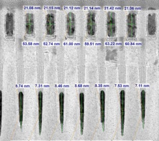
Today’s Helios 5 DualBeam line of instruments redefine analysis on even the smallest, most complex structures by combining precise sample modification with ultra high-resolution imaging. These instruments offer fast, easy, and high-quality sample preparation for scanning/transmission electron microscopy (S/TEM) imaging, and advanced automation capabilities that dramatically speed time to results.
For example, the Helios 5 PXL PFIB Wafer DualBeam changes the game by reducing time-to-data from days to hours for in-line, through-stack metrology and structural verification of 3D NAND and other high-aspect ratio structures. Likewise, the Helios 5 EXL DualBeam is the first microscope in the semiconductor industry that utilizes machine learning to expedite and automate wafer sample preparation for transmission electron microscope (TEM) imaging and analysis.
Today’s TEM line of instruments continues to set the standard for (S)TEM analysis and characterization for a wide range of advanced structures and materials at atomic-scale resolution. For example, the Spectra Ultra includes a new energy-dispersive X-Ray (EDX) analysis system, the Thermo Scientific Ultra-X, with the largest detector area available in a commercially released (S)TEM. Combined with the new objective lens design, the EDX detector architecture makes it possible to capture X-Rays twice as fast, enabling the analysis of more beam-sensitive materials and samples with previously undetectably low concentrations of trace elements.
An ongoing commitment to partnership and innovation
Over the coming years, the demand for semiconductors is expected to continue its exponential growth as new innovations take hold, and industries require semiconductors that deliver higher performance, energy efficiency, and reliability.
As semiconductor manufacturers work to meet these demands, semiconductor metrology, failure analysis, and characterization will take on an even greater role in the product development process—and Thermo Fisher plans to meet these needs.
By continuing our investments in leading-edge solutions, our goal is to help the semiconductor industry accelerate its own advances well into the future. And as we reflect on the past 40 years of semiconductor progress, ultimately this joint spirit of innovation has defined our mutual success.
To learn more about our role in the history of semiconductor engineering, please see our fact sheet, Thermo Fisher: 40 Years of Semiconductor Analysis Innovation.


—
David Akerson is a Sr. Global Market Development Manager at Thermo Fisher Scientific.
Revolutionizing the way TEM metrology data is collected
As I discussed in my 2024 year-end article, the semiconducto...
Read MoreSemiconductor Nanoprobing Boosts TEM Analysis Success Rates on Advanced Logic Devices
Growing need for semiconductor nanoprobing As the semiconduc...
Read More
Accelerating Semiconductor Device Analysis with the Power of the Helios 5 EXL Wafer DualBeam
Semiconductor fabrication challenges Semiconductor fabricati...
Read MoreFailure analysis of wide bandgap semiconductor devices
Compound semiconductors create analytical challenges Our eve...
Read More
Leave a Reply