3D semiconductor packaging industry insights from Semicon Korea 2023
This February was my first time in Seoul. There were more than 57,000 attendees at Semicon Korea and more than 2,000 companies exhibiting their latest innovations to help advance semiconductor technologies in a post-pandemic era. I was really impressed by one of the keynote speeches in particular, delivered by Dr. Eric Beyne from IMEC on 3D semiconductor packaging technology.
As explained by Dr. Beyne, modern electronic systems are becoming increasingly complex. It is becoming progressively challenging for two-dimensional device scaling to deliver higher system performance and to continuously extend Moore’s Law. Therefore, 3D semiconductor packaging and heterogeneous integration have become a necessary and sustainable approach to provide higher bandwidth, reduced power consumption, and overall performance improvements of the system, which is especially critical for portable electronics.
3D heterogeneous integration and advanced semiconductor packaging
3D packaging is a complicated process, which includes multiple steps, such as wafer fabrication, wafer thinning, wafer bonding, etc. Connecting multiple dies and wafers stacked on top of each other is increasingly reliant on through-silicon-via (TSV) technology to achieve performance gains without using traditional wire-bond assembly. The benefits of using TSVs encompass smaller layout space, higher signal performance, and reduced power consumption.
Today’s modern semiconductor packaging structure incorporates thousands of TSVs to connect multiple chips as shown in Figure 1. For example, High Bandwidth Memory (HBM) is one of the very early techniques that utilized TSVs to achieve heterogeneous integration of multiple memory chips. The HBM2 introduced in 2019 has 12 stacked chips with 60,000 TSVs as the interconnection [1].

Figure 1. A stack of multiple chips integrated using TSVs
TSV process metrology and defect analysis challenges
Fabricating the TSVs is a demanding process as illustrated in Figure 2. The process includes several critical steps, such as TSV etch, liner/barrier deposition, TSV fill, and chemical mechanical polish (CMP). Each process module has its own metrology, defect inspection and analysis challenges. Unfortunately, current metrology solutions, such as CD-SEM or traditional optical CD (OCD), are challenged to automatically and precisely measure TSV CDs buried in the high-aspect-ratio (HAR) structure.
For instance, the liner and barrier layers of the TSVs are fabricated with thin film deposition processes that are in the nanometer scale. For this process, precise measurement and control of these critical dimensions (CDs) requires high-resolution Scanning Electron Microscopy (SEM) images on the cross sections of the TSVs.

Figure 2. TSV fabrication process with increasing demand on metrology, defect inspection and analysis workflows
Similarly, the shrinkage of the TSV structures has made it likely that nanometer-size structural voids or process defects, as described in Figure 2, may be hidden in the complex 3D structures that cannot be detected and analyzed by the current inspection tools, such as Scanning Acoustic Microscopy (SAM) or IR microscopy [2].
As these techniques usually only detect structural defects at the micrometer scale, high-voltage SEMs have become a useful technique for detecting and analyzing small structural defects at the nanometer scale. However, the SEM is still limited by its information depth, especially when faced with the stacking structure of the TSVs as shown in Figure 3 [2].

Figure 3. Small structural defects hidden in TSV stacks (TSV process defects, micro-bump defects, Cu-Cu hybrid bonding defects, TSV misalignment, etc.)
TSV stacking challenges
The stacking of the TSVs causes additional challenges due to the increasing aspect ratio of the structure and the total thickness of the stack, which can be in the range of hundreds of micrometers or more.
Further complicating TSV stacking challenges is, as explained by Dr. Beyne, the increasing number of stacked chips and the complexity of the interconnections which will require higher density TSV arrays with smaller critical dimensions (CD) and pitch sizes to be built in the 3D structure. As a result, the likelihood of nanometer-size defects or voids from TSV process, micro-bump and hybrid bonding defects, die-to-wafer (D2W) and wafer-to-wafer (W2W) overlays, and TSV misalignments is expected to increase.
For example, small defects can be hidden in the bonding materials, as a result of micro-bump or dielectric underfill. With the TSV pitch sizes shrinking, Cu-Cu hybrid bonding process are expected to replace the current micro-bumping technique as shown in Figure 3. Therefore, being able to identify potential issues such as Cu-Cu interfacial voids and TSV misalignments will become critical for the entire process yield.
To efficiently analyze buried, nanometer-scale defects in hundreds-of-micrometer tall structures requires not only high-throughput material removal, but also high-resolution imaging of the 3D volume capturing subtle details. And as die-to-wafer and wafer-to-wafer level packaging increases, it is also accelerating demand for these metrology and analytical capabilities to become available on full wafers.
Wafer level metrology and defect analysis
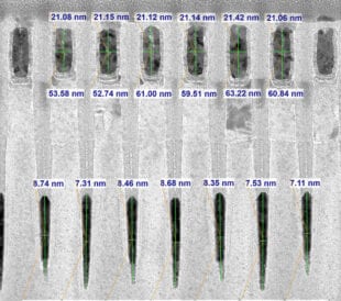
The Thermo Scientific Helios 5 PXL DualBeam is a 300mm-wafer-level dual beam system with both plasma focused ion beam (PFIB) and scanning electron microscope (SEM). The Xe+ PFIB enables high-throughput material removal to make cross sections on the TSV structures for metrology and defect analysis. The milling acuity and built-in “rocking polish” capability provides “curtain-free” cross sectioning on the HAR structure of the TSVs for high-resolution SEM imaging as shown in Figure 4. The tilting stage makes the PFIB cross-sectioning to SEM imaging a seamless high-efficiency workflow.

Figure 4. High-resolution SEM images on TSV cross sections with (a) metrology of TSVs and bonding structures, and (b) with structural defects and TSV misalignments
The system is also capable of taking a series of SEM images while slicing through TSV stacks. The series of SEM images can then be reconstructed into a 3D dataset using Thermo Scientific Avizo Software for defect inspection and analysis as shown in Figure 5. This capability provides an excellent solution to the current gap of inspecting and analyzing deeply buried small defects in highly-complex-stack structures of 3D packaging.

Figure 5. 3D reconstruction of TSV with segmentations showing Cu fill (violet), liner/barrier layers (blue), and voids (green).
To learn more about advanced semiconductor packaging applications on Helios 5 PXL DualBeam, watch our related on-demand SPARK webinar, presented by Dr. Ivy Wu.
Thermo Fisher Scientific provides process metrology, defect inspection, and failure analysis solutions at both wafer level and die level for advanced packaging industry. Visit our previous SPARK webinars to learn more.
[1]. Mark Lapedus, What’s Next for High Bandwidth Memory
[2]. Cong Chen et. al., “Detection of Bonding Voids for 3D Integration”, SPIE Advanced Lithography + Patterning Conference, 2023

Revolutionizing the way TEM metrology data is collected
As I discussed in my 2024 year-end article, the semiconducto...
Read MoreSemiconductor Nanoprobing Boosts TEM Analysis Success Rates on Advanced Logic Devices
Growing need for semiconductor nanoprobing As the semiconduc...
Read More
Accelerating Semiconductor Device Analysis with the Power of the Helios 5 EXL Wafer DualBeam
Semiconductor fabrication challenges Semiconductor fabricati...
Read MoreFailure analysis of wide bandgap semiconductor devices
Compound semiconductors create analytical challenges Our eve...
Read More
Leave a Reply