Search Thermo Fisher Scientific
Thermo Scientific™
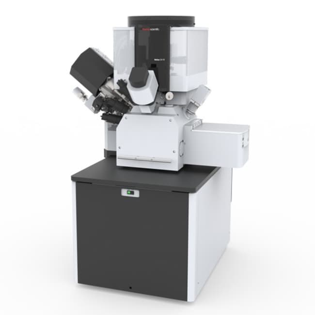
Helios™ G4 PFIB HXe DualBeam™ for Semiconductors
Katalognummer: HELIOSG4HXE

Thermo Scientific™
Helios™ G4 PFIB HXe DualBeam™ for Semiconductors
Katalognummer: HELIOSG4HXE
The Thermo Scientific™ Helios™ G4 PFIB HXe DualBeam System provides unique capabilities to enable damage-free delayering of 10nm semiconductor devices and advanced failure analysis of 3D packages, in addition to a wide range of other large area FIB processing applications.
1 von 1 wird angezeigt
| Katalognummer | Spezifikationen | Packungsgröße | Preis (EUR) | ||||||||||||||||||||||||||||||||||||||||||||||||||||||||||||||||||||||||||||||||||||||||||||||||||||
|---|---|---|---|---|---|---|---|---|---|---|---|---|---|---|---|---|---|---|---|---|---|---|---|---|---|---|---|---|---|---|---|---|---|---|---|---|---|---|---|---|---|---|---|---|---|---|---|---|---|---|---|---|---|---|---|---|---|---|---|---|---|---|---|---|---|---|---|---|---|---|---|---|---|---|---|---|---|---|---|---|---|---|---|---|---|---|---|---|---|---|---|---|---|---|---|---|---|---|---|---|---|---|---|
| HELIOSG4HXE | - | Angebot anfordern | |||||||||||||||||||||||||||||||||||||||||||||||||||||||||||||||||||||||||||||||||||||||||||||||||||||
| |||||||||||||||||||||||||||||||||||||||||||||||||||||||||||||||||||||||||||||||||||||||||||||||||||||||
The Helios G4 PFIB HXe DualBeam System enables you to:
- Reveal the finest details using best-in-class Elstar™ SEM Electron Column with high-current UC+ monochromator technology, enabling nanometer SEM image resolution and surface sensitivity.
- Perform the highest throughput and quality relevant 3D characterization, cross-sectioning, and micromachining using the next-generation 2.5μA Xenon Plasma FIB (PFIB 2.0) Column.
- Achieve high-productivity, curtain-free preparation of large area cross-sections and highest quality TEM lamella with Auto Rocking Mill.
- Achieve exceptional low-kV ion beam performance, enabling material sensitivity and low sample preparation damage.
- Experience the most advanced capabilities for electron and ion beam induced deposition and etching on FIB-SEM systems with the optional MultiChem or GIS gas delivery systems.
- Deprocessing, with proprietary Dx and DE chemistries, of copper metallization in regular and low-k dielectrics. And milling advanced packaging materials with plasma FIB-based chemistries and recipes.
Abbildungen
Dokumente und Downloads
Zertifikate
Nach Chargennummer oder Teil-Chargennummer suchen
Häufig gestellte Fragen (FAQ)
Zitierungen und Referenzen
Search citations by name, author, journal title or abstract text