Search Thermo Fisher Scientific

c7c8 - Key/Specs/Resources/Appl/Tech/Doc/Contact
Spectra Ultra Scanning Transmission Electron Microscope
To truly optimize TEM and STEM imaging, EDX and EELS may require acquisition of different signals at different accelerating voltages. The rules may vary from sample to sample but, it is generally accepted that: 1) the best imaging is done at the highest possible accelerating voltage above which visible damage will occur, 2) EDX, especially when mapping, benefits from lower voltages with increased ionization cross-sections, thus yielding better signal-to-noise ratio maps for a given total dose, and 3) EELS works best at high voltages to avoid multiple scattering, which degrades the EELS signal with increasing sample thickness.
Unfortunately, acquisition at different accelerating voltages on the same sample without losing the region of interest—all during a single microscopy session—is not possible. At least, until now.
Imagine a Thermo Scientific Spectra 300 S/TEM:
- That can truly be operated at different voltages (all the voltages between 30 and 300 kV for which alignments were purchased) in a single microscopy session
- Where changing from an accelerating voltage to any other one takes about 5 minutes
- That can accommodate a radically different EDX concept with a 4.45 srad solid angle (4.04 srad solid angle with an analytical double tilt holder)
With the new Spectra Ultra S/TEM, the accelerating voltage becomes an adjustable parameter, just like probe current, and the massive Ultra-X EDX system enables chemical characterization of materials too beam-sensitive for conventional EDX analysis.
The Spectra Ultra aberration-corrected S/TEM offers an industry leading level of characterization capabilities for materials science and semiconductor applications at the highest resolution on a wide variety of samples.
Built on an ultra-stable foundation
The Spectra Ultra S/TEM is delivered on a platform designed to offer an unprecedented level of mechanical stability quality through passive and (optional) active vibration isolation.
Like the Thermo Scientific Spectra 200 S/TEM and Spectra 300 S/TEM, the system is housed in a fully redesigned enclosure with a built-in on-screen display for convenient specimen loading and removal. For the first time, full modularity and upgradeability can be offered between uncorrected and single-corrected configurations with variable heights, allowing maximum flexibility for different room configurations.
Fastest time to optimized results from more materials
The ability to switch accelerating voltage and achieve ultimate stability of the optics and specimen stage in less than five minutes provides unique capabilities and a new, faster way to operate the microscope to extract optimized information from your specimen.
- The highest resolution spatial information (50 pm) from a specimen can be collected at 300 kV. Then, the system can be switched to lower accelerating voltages for STEM EDX mapping with increased ionization cross sections from the same area with higher X-ray yields, leading to reduced sample damage.
- For specimens that suffer from “knock-on” damage, the accelerating voltage can be switched multiple times within a single microscopy session to mitigate beam damage and ensure data integrity is maintained.
This capability is achieved by the introduction of a radically redesigned objective lens that can operate at constant power for all accelerating voltages between 30 and 300 kV.

Stabilization of the stage after a switch from 60 to 300 kV.
The constant power concept was pioneered with the introduction of the Titan TEM, formerly produced by FEI, over a decade and a half ago. It enabled mode switching at any given, but fixed, accelerating voltage without inducing drift because the objective lens thermal load would remain constant. Now, this concept has been extended to all voltage changes between 30 and 300 kV.
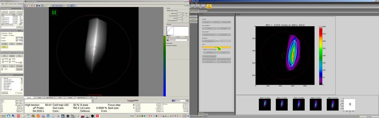
The objective lens produces magnetic fields that vary wildly depending on the mode and accelerating voltage. However, for the Spectra Ultra (S)TEM’s new objective lens, the thermal load remains constant at all times. The stabilization time of the optics and stage when switching between different accelerating voltages has been reduced from several hours to less than five minutes.
The benefits of accelerating voltage flexibility in combination with the Ultra-X detector are clear. Fast and flexible control over the HT, in combination with Ultra-X, opens the gateway to fast imaging at the highest resolution in combination with optimized STEM EDX analysis of beam-sensitive materials.
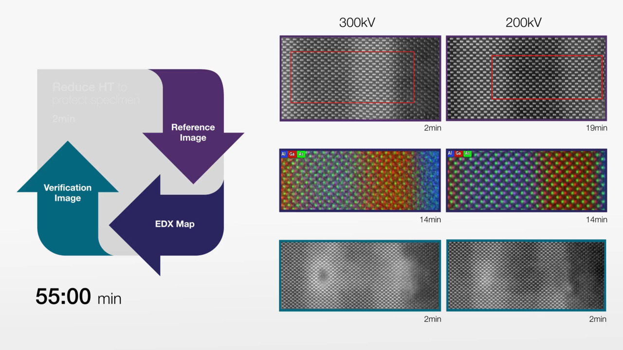
The benefit of accelerating voltage flexibility in combination with Ultra-X. STEM EDX mapping at two accelerating voltages in less than one hour. Beam-induced specimen damage at 300 kV is seen in an InAlGaAs layered specimen. By lowering the accelerating voltage to 200 kV, the beam-induced specimen damage is reduced and the EDX map is visibly improved. Specimen courtesy of J. Zweck, University of Regensburg.
Lowest dose STEM/EDX for the characterization of more materials
The Spectra Ultra S/TEM brings the next era in EDX detection to the market with our Ultra-X EDX detector. Providing a solid angle (>4.45 Sr) at least two times greater than any other EDX detector solution, the sensitivity of Ultra-X opens up new capabilities in STEM EDX analysis. Even with the shadowing of an analytical double tilt holder considered, the solid angle is >4.04 srad

Figure 2. Normalized count-rates as function of tilt angle for a single detector, Super-X, Dual-X, and the new Ultra-X. Data was recorded at 200 kV with optimized specimen holders for each detector configuration. Zaluzec, et al. Submitted to Microscopy and Microanalysis, 2021.
The benefits of such high sensitivity are shown in the improvement in spectrum imaging quality with Ultra-X. A comparison using the same electron dose (8.28 x 10⁸ e/Å2) is shown between Super-X, Dual-X, and Ultra-X on a DyScO3 specimen. The improvements in the signal-to-noise ratio shown in the raw data can be easily seen. Additionally, the oxygen lattice can be directly imaged with Ultra-X, where it could not with Super-X and Dual-X.

Figure 3. A quantitative comparison is shown between Super-X, Dual-X, and Ultra-X on a DyScO3 specimen. The improvements in the signal-to-noise ratio are clearly seen. Specimen courtesy of L.F. Kourkoutis, Cornell University.
Additionally, the high sensitivity of Ultra-X means that the same level of chemical information can be obtained with a fraction of the electron dose that would be required for other EDX detector solutions. This opens up possibilities for STEM EDX analysis from more beam-sensitive specimens and faster mapping for more stable specimens.

Figure 4. Comparable line profiles extracted from the spectrum images demonstrate that a similar signal-to-noise ratio can be obtained with Ultra-X with only a fraction of the electron dose needed for Super-X. Specimen courtesy of L.F. Kourkoutis, Cornell University.
Unprecedented sensitivity with the Panther STEM detection system
STEM imaging on the Spectra Ultra S/TEM has been reimagined with the Panther STEM detection system, which includes a new data acquisition architecture and two new, solid-state, eight-segment ring and disk STEM detectors (16 segments in total). The new detector geometry offers access to advanced STEM imaging capability combined with the sensitivity to measure single electrons.
 proving the excellent homogeneity of sensitivity across the segments.")
Scanning image of the 16 segmented ring and disk detectors with an intensity profile (in red) proving the excellent homogeneity of sensitivity across the segments.
The entire signal chain is optimized and tuned to provide unprecedented signal-to-noise imaging capability with extremely low doses to facilitate imaging of beam-sensitive materials. Additionally, the completely redeveloped data acquisition infrastructure can combine different individual detector segments, with the future possibility of combining detector segments in arbitrary ways, generating new STEM imaging methods and revealing information that is not present in conventional STEM techniques. The architecture is also scalable and provides an interface to synchronize multiple STEM and spectroscopic signals.
 images of SrTiO₃.")
Comparison SrTiO₃ [001] HAADF images taken with the Panther STEM detection system with 3 pA, 1.3 pA and <1 pA of probe current. Even with probe currents <1 pA, the signal-to-noise ratio in the image allows automation routines like OptiSTEM+ to correct 1st and 2nd order aberrations in the probe forming optics, delivering sharp images.

Extreme low-dose imaging of the metal organic framework (MOF) UiO 66. A probe current of <0.5 pA was used in combination with iDPC and the Panther STEM detection system to image atomic-level details in this highly dose-sensitive material with a spatial resolution of 1.4 Å. The image is a single shot with a frame time of 23.5 seconds. Specimen courtesy of Professor Y. Han, King Abdullah University of Science and Technology. (Data acquired on a Spectra 300 TEM.)
Highest resolution STEM imaging performance
The Spectra Ultra S/TEM is equipped with the new S-TWIN' (S-TWIN Prime) pole piece. The S-TWIN' is based on the S-TWIN design. It provides both ultra-high spatial resolution in STEM (e.g., 50 pm at 300 kV and 96 pm at 60 kV) and a wide gap for experiments requiring large tilt angles or bulky in situ holders.
The S-TWIN' differs in its ability to support an extremely high solid-angle EDX solution (see section on Ultra-X) without compromising spatial resolution. The S-TWIN', in combination with the enhanced mechanical stability of the base and the latest S-CORR probe corrector, matches the combined spatial resolution and combined high probe current specifications of the Spectra 300 TEM.
For a full list of these specifications—the highest commercially-available STEM specifications—please refer to the Spectra Ultra S/TEM datasheet.
High-energy resolution and high-brightness sources
X-FEG/Mono or X-FEG/UltiMono
The Spectra Ultra S/TEM can be optionally equipped with either a standard monochromator (X-FEG/Mono) or a high-energy resolution monochromator (X-FEG/UltiMono). Both monochromators are automatically excited and tuned with single-click operation to achieve the highest energy resolution possible on each configuration by using OptiMono or OptiMono+, respectively.
The X-FEG/Mono can be automatically tuned from 1 eV down to 0.2 eV, while the X-FEG/UltiMono can be automatically tuned from 1 eV down to <25 meV.
Both sources can be operated from 30 to 300 kV to accommodate the widest range of specimens. Both can also be run in standard mode, with the monochromators switched off, to accommodate experiments that require high brightness, including STEM EDS mapping, ultra-high-resolution STEM, or high total current, such as TEM imaging, all with no compromise to the other specifications of the system. This flexibility gives the Spectra Ultra (S)TEM the capability to function in settings where a large range of experiments are expected to be performed on one system.
OptiMono+ exciting an X-FEG/UltiMono from the monochromator off state (with 1 eV energy resolution) to the monochromator fully excited state (<30 meV) at 60 kV. (Data acquired on a Spectra 300 TEM.)
X-CFEG
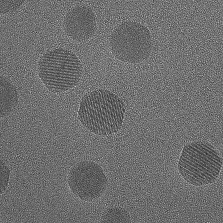
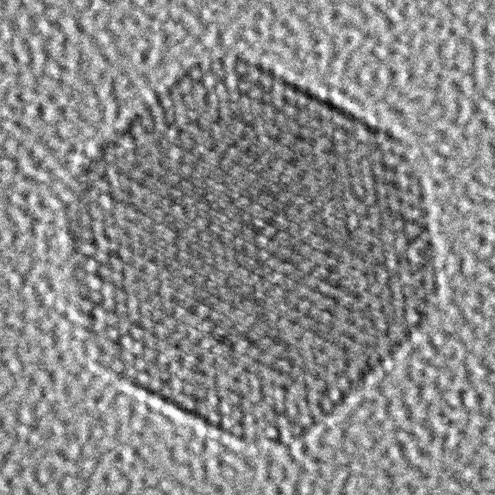
The Spectra Ultra S/TEM can optionally be powered by a new cold field emission gun (X-CFEG). The X-CFEG has extremely high brightness (>>1.0 x 10⁸ A/m2/Sr/V*), low energy spread (<0.4 eV), and can operate from 30 to 300 kV. This provides simultaneous high-resolution STEM imaging with high probe currents for high throughput, fast acquisition STEM analytics in parallel with high-energy resolution. With the powerful combination of X-CFEG and the S-CORR probe aberration corrector, sub-Angstrom (<0.8 Å) STEM-imaging resolution with over 1,000 pA of probe current can be routinely achieved.
 images of silicon.")
Si[110] HAADF images taken with the X-CFEG/S-CORR combination; probe currents range from 0.016 nA (left) up to 1 nA (right) while maintaining <76 pm STEM resolution.
Further, probe currents can be flexibly tuned from <1 pA up to the nA range with fine control of the gun and condenser optics, all with minimum impact on the probe aberrations, so that the widest range of specimens and experiments can be accommodated.
As with all cold field emission sources, the sharp tip requires a periodic regeneration (called flashing) to maintain the probe current. With the X-CFEG, the tip only requires flashing once per working day, a process takes less than a minute. There is no measurable impact on the probe aberrations even in the highest resolution imaging conditions, and the daily tip flashing process has no impact on the tip lifetime.
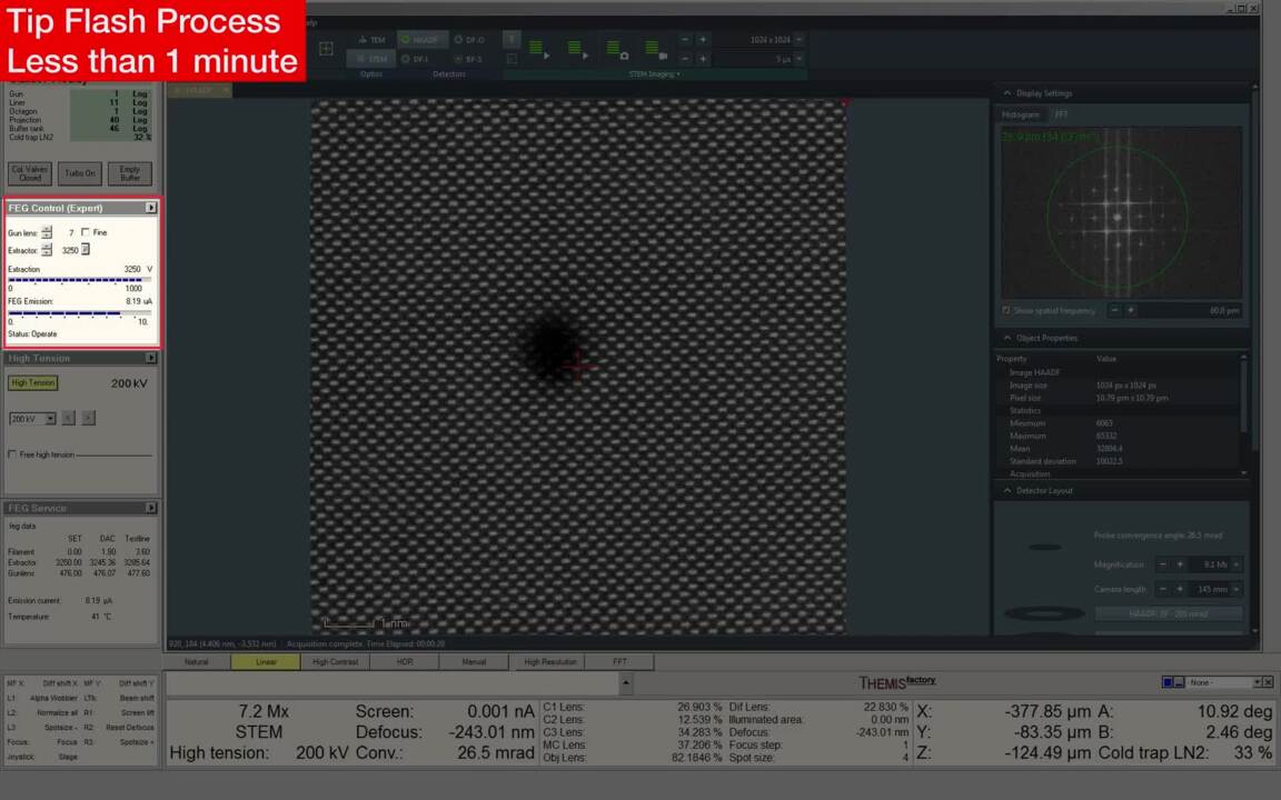
Tip flashing on the X-CFEG: 60 pm resolution at 200 kV is maintained before and after tip flashing without adjustment of the optics. The process takes <1 min, is required only once per working day, and has no impact on the lifetime of the tip.
This new generation X-CFEG also produces enough total beam current (>14 nA) to support standard TEM imaging experiments (e.g. in situ) with large parallel probes, making it a uniquely all-purpose, yet high performance, C-FEG.
Adding to the flexible nature of the X-CFEG is the capability to adjust the energy resolution by varying the extraction voltage.
In the example below, the energy resolution was adjusted between 0.39eV, with <500pA of probe current and 0.31eV, with >300pA of probe current. Maintaining high probe currents with high energy resolution allows for detailed analysis of Energy Loss Near Edge Structure (ELNES) analysis without the need for a monochromator on core loss edges. The spatial resolution, as demonstrated in the HAADF image of DyScO3, remains unaffected (in this case <63pA) which means that STEM EELS experiments with simultaneously high spatial resolution, energy resolution and signal to noise ratio can now be performed.
The lifetime of the tip is unaffected by the extraction voltage chosen to perform the experiment.

The energy resolution of the ultra-high brightness X-CFEG can be adjusted using the extraction voltage. In the case above it was varied between 0.39eV (with <500pA of probe current) and 0.31eV (with >300pA of probe current). The spatial resolution, as demonstrated in the HAADF image of DyScO3, remains unaffected (in this case <63pA).
Sample courtesy Professor L.F. Kourkoutis, Cornell University
Advanced STEM imaging capabilities
The Spectra Ultra S/TEM can be configured with an electron microscope pixel array detector (EMPAD) or a Thermo Scientific Ceta™ Camera with speed enhancement to collect 4D STEM data sets.
The EMPAD is capable of 30–300 kV and provides a high dynamic range (1:1,000,000 e- between pixels), high signal- to-noise ratio (1/140 e-), and high speed (1,100 frames per second) on a 128x128 pixel array, which makes it the optimal detector for 4D STEM applications (e.g., where the details of the central and diffracted beams need to be analyzed simultaneously, as in the following ptychography image).
More details can be found in the EMPAD datasheet.
 image of MoS₂")
The EMPAD detector can be used for a wide variety of applications. On the left, it is used to extend spatial resolution (0.39 Å) beyond the aperture limited resolution at low accelerating voltages (80 kV) in a bi-layer of the 2D material MoS₂ ( Jiang, Y. et al. Nature 559, 343–349, 2018). On the right, it is used to independently image dark field reflections, revealing the complex microstructure of the precipitates in a superalloy (Sample courtesy Professor G. Burke, University of Manchester).
The Ceta Camera with speed enhancement offers an alternative for 4D STEM applications where a greater number of pixels is required and when EDS analysis needs to be combined with each point in the STEM scan. This solution provides higher resolution diffraction patterns (up to 512 x 512 pixel resolution), suited for applications such as strain measurement.
In situ capabilities of the Spectra Ultra S/TEM
The Spectra Ultra S/TEM accepts a wide range of holders for in situ experiments with its all-in-one S-TWIN’ wide-gap pole piece. The family of Thermo Scientific NanoEx Holders can be seamlessly integrated with the microscope, enabling MEMS device-based heating for atomic imaging at elevated temperatures. Below, gold nanoparticles are heated to 700 degrees Celsius and the resulting motion is captured simultaneously with full frame 4k by 4k pixel resolution at a rate greater than 30 frames per second on a Ceta Camera with speed enhancement. The result is high spatial and temporal resolution of highly dynamic molecular behavior.
On the left is a high frame rate movie of gold nano-islands at high temperature, collected on a Ceta Camera with speed enhancement. On the right, the 4k x 4k sensor allows digital zoom while maintaining high resolution in the field of interest.
Style Sheet to change H2 style to p with em-h2-header class

On-Demand Webinar: Expanding the horizons of materials analysis with (S)TEM and EDX
(S)TEM, (scanning) transmission electron microscopy, and EDX, energy dispersive X-ray spectroscopy, are complimentary techniques that allow you to characterize the structural and chemical composition of materials down to the atom.
View our two-part on-demand webinar to learn about advances in (S)TEM and EDX that have enabled the analysis of the widest range of materials to date, including challenging samples such as beam-sensitive materials.
Uncorrected |
|
Probe corrected |
|
Probe+Image Corrected X-FEG/Mono |
|
Probe+Image Corrected X-FEG/UltiMono |
|
Probe+Image Corrected X-CFEG |
|
Source |
|
Style Sheet for Products Table Specifications

Incredible catalysis.

More answers with ETEM
OptiMono+ exciting an X-FEG/UltiMono from the monochromator off state (with 1 eV energy resolution) to the monochromator fully excited state (<30 meV) at 60 kV.
Tip flashing on the X-CFEG: 60 pm resolution at 200 kV is maintained before and after tip flashing without adjustment of the optics. The process takes <1 min, is required only once per working day, and has no impact on the lifetime of the tip.
On the left is a high frame rate movie of gold nano-islands at high temperature, collected on a Ceta Camera with speed enhancement. On the right, the 4k x 4k sensor allows digital zoom while maintaining high resolution in the field of interest.

The benefit accelerating voltage flexibility in combination with Ultra-X. Beam induced specimen damage at high accelerating voltages is seen in an InAlGaAs layered specimen. By reducing the accelerating voltage, both the beam induced specimen damage and the MMF are dramatically reduced.

The 16 segmented ring and disk detectors of the Panther STEM detection system allow for a range of STEM signals without the need for multiple detectors.

Comparison SrTiO₃ [001] HAADF images taken with the Panther STEM detection system with 3 pA, 1.3 pA and <1 pA of probe current. Even with probe currents <1 pA, the signal-to-noise ratio in the image allows automation routines like OptiSTEM+ to correct 1st and 2nd order aberrations in the probe forming optics, delivering sharp images.
 UiO 66. A probe current of <0.5 pA was used in combination with iDPC and the Panther STEM detection system to image atomic level details in this highly dose-sensitive material with a spatial resolution of 1.4 Å. The image is a single shot with a frame time of 23.5 seconds (Specimen courtesy of Professor Y. Han, King Abdullah University of Science and Technology).")
Extreme low-dose imaging of the metal organic framework (MOF) UiO 66. A probe current of <0.5 pA was used in combination with iDPC and the Panther STEM detection system to image atomic level details in this highly dose-sensitive material with a spatial resolution of 1.4 Å. The image is a single shot with a frame time of 23.5 seconds (Specimen courtesy of Professor Y. Han, King Abdullah University of Science and Technology).
 images of silicon.")
Si[110] HAADF images taken with the X-CFEG/S-CORR combination; probe currents range from 0.016 nA (left) up to 1 nA (right) while maintaining <76 pm STEM resolution.
 and 0.31eV (with >300pA of probe current). The spatial resolution, as demonstrated in the HAADF image of DyScO3, remains unaffected (in this case <63pA). Sample courtesy Professor L.F. Kourkoutis, Cornell University")
The energy resolution of the ultra-high brightness X-CFEG can be adjusted using the extraction voltage. In the case above it was varied between 0.39eV (with <500pA of probe current) and 0.31eV (with >300pA of probe current). The spatial resolution, as demonstrated in the HAADF image of DyScO3, remains unaffected (in this case <63pA). Sample courtesy Professor L.F. Kourkoutis, Cornell University
 images of MoS₂.")
The EMPAD detector can be used for a wide variety of applications. On the left, it is used to extend spatial resolution (0.39 Å) beyond the aperture limited resolution at low accelerating voltages (80 kV) in a bi-layer of the 2D material MoS₂ (Jiang, Y. et al. Nature 559, 343–349, 2018). On the right, it is used to independently image dark field reflections, revealing the complex microstructure of the precipitates in a superalloy (Sample courtesy Professor G. Burke, University of Manchester).
TEM and EDX")
Expanding the horizons of materials analysis with (S)TEM and EDX
(S)TEM, (scanning) transmission electron microscopy, and EDX, energy dispersive X-ray spectroscopy, are complimentary techniques that allow you to characterize the structural and chemical composition of materials down to the atom.
View our two-part on-demand webinar to learn about advances in (S)TEM and EDX that have enabled the analysis of the widest range of materials to date, including challenging samples such as beam-sensitive materials.
Incredible catalysis.
More answers with ETEM
OptiMono+ exciting an X-FEG/UltiMono from the monochromator off state (with 1 eV energy resolution) to the monochromator fully excited state (<30 meV) at 60 kV.
Tip flashing on the X-CFEG: 60 pm resolution at 200 kV is maintained before and after tip flashing without adjustment of the optics. The process takes <1 min, is required only once per working day, and has no impact on the lifetime of the tip.
On the left is a high frame rate movie of gold nano-islands at high temperature, collected on a Ceta Camera with speed enhancement. On the right, the 4k x 4k sensor allows digital zoom while maintaining high resolution in the field of interest.
The benefit accelerating voltage flexibility in combination with Ultra-X. Beam induced specimen damage at high accelerating voltages is seen in an InAlGaAs layered specimen. By reducing the accelerating voltage, both the beam induced specimen damage and the MMF are dramatically reduced.
The 16 segmented ring and disk detectors of the Panther STEM detection system allow for a range of STEM signals without the need for multiple detectors.
Comparison SrTiO₃ [001] HAADF images taken with the Panther STEM detection system with 3 pA, 1.3 pA and <1 pA of probe current. Even with probe currents <1 pA, the signal-to-noise ratio in the image allows automation routines like OptiSTEM+ to correct 1st and 2nd order aberrations in the probe forming optics, delivering sharp images.
Extreme low-dose imaging of the metal organic framework (MOF) UiO 66. A probe current of <0.5 pA was used in combination with iDPC and the Panther STEM detection system to image atomic level details in this highly dose-sensitive material with a spatial resolution of 1.4 Å. The image is a single shot with a frame time of 23.5 seconds (Specimen courtesy of Professor Y. Han, King Abdullah University of Science and Technology).
Si[110] HAADF images taken with the X-CFEG/S-CORR combination; probe currents range from 0.016 nA (left) up to 1 nA (right) while maintaining <76 pm STEM resolution.
The energy resolution of the ultra-high brightness X-CFEG can be adjusted using the extraction voltage. In the case above it was varied between 0.39eV (with <500pA of probe current) and 0.31eV (with >300pA of probe current). The spatial resolution, as demonstrated in the HAADF image of DyScO3, remains unaffected (in this case <63pA). Sample courtesy Professor L.F. Kourkoutis, Cornell University
The EMPAD detector can be used for a wide variety of applications. On the left, it is used to extend spatial resolution (0.39 Å) beyond the aperture limited resolution at low accelerating voltages (80 kV) in a bi-layer of the 2D material MoS₂ (Jiang, Y. et al. Nature 559, 343–349, 2018). On the right, it is used to independently image dark field reflections, revealing the complex microstructure of the precipitates in a superalloy (Sample courtesy Professor G. Burke, University of Manchester).
Expanding the horizons of materials analysis with (S)TEM and EDX
(S)TEM, (scanning) transmission electron microscopy, and EDX, energy dispersive X-ray spectroscopy, are complimentary techniques that allow you to characterize the structural and chemical composition of materials down to the atom.
View our two-part on-demand webinar to learn about advances in (S)TEM and EDX that have enabled the analysis of the widest range of materials to date, including challenging samples such as beam-sensitive materials.
Style Sheet to change Applications H3 to p with em-h3-header class
Style Sheet to change H3 to p with em-h3-header class

Control de procesos mediante microscopía electrónica
La industria moderna exige un alto rendimiento con una calidad superior, un equilibrio que se mantiene a través de un control de procesos sólido. Las herramientas SEM y TEM con software de automatización exclusivo proporcionan información rápida y multiescala para la supervisión y la mejora de procesos.

Control de calidad y análisis de fallos
El control y garantía de calidad son esenciales en la industria moderna. Ofrecemos una gama de herramientas de EM y espectroscopía para el análisis multiescala y multimodal de defectos, lo que le permite tomar decisiones fiables e informadas para el control y la mejora de procesos.

Investigación sobre materiales fundamentales
Se investigan nuevos materiales a escalas cada vez más pequeñas para lograr el máximo control de sus propiedades físicas y químicas. La microscopía electrónica proporciona a los investigadores información clave sobre una amplia variedad de características materiales a escala nanométrica.

Desarrollo y trazabilidad de semiconductores
Microscopía electrónica avanzada, haz de iones enfocado y técnicas analíticas asociadas para identificar soluciones viables y métodos de diseño para la fabricación de dispositivos semiconductores de alto rendimiento.
Style Sheet for Komodo Tabs

Espectroscopia de energía dispersiva
La espectroscopía de energía dispersiva (EDS) recopila información elemental detallada junto con imágenes de microscopía electrónica, proporcionando un contexto de composición esencial para las observaciones de EM. Con EDS, se puede determinar la composición química desde barridos de superficie rápidos y holísticos hasta átomos individuales.
_Technique_800x375_144DPI.jpg)
Tomografía EDS en 3D
La investigación de materiales modernos depende cada vez más del análisis a nanoescala en tres dimensiones. La caracterización en 3D, incluidos los datos de composición para el contexto químico y estructural completo, es posible con EM en 3D y espectroscopia de rayos X dispersiva.

Asignación elemental a escala atómica con EDS
El EDS de resolución atómica proporciona un contexto químico incomparable para el análisis de materiales al diferenciar la identidad elemental de los átomos individuales. Cuando se combina con TEM de alta resolución, es posible observar la organización precisa de los átomos en una muestra.
_Technique_800x375_144DPI.jpg)
Análisis elemental EDS
EDS proporciona información de composición vital sobre las observaciones de microscopio electrónico. En concreto, nuestros exclusivos sistemas de detectores Super-X y Dual-X añaden opciones para mejorar el rendimiento y/o la sensibilidad, permitiendo optimizar la adquisición de datos para cumplir con sus prioridades de investigación.

Espectroscopía de pérdida de energía de electrones
La investigación en ciencias de los materiales se beneficia de la EELS de alta resolución para una amplia gama de aplicaciones analíticas. Esto incluye asignación elemental de alto rendimiento, alta relación señal-ruido, así como sondeo de estados de oxidación y fonones de superficie.

Experimentación in situ
La observación directa y en tiempo real de los cambios microestructurales con microscopía electrónica es necesaria para comprender los principios subyacentes de los procesos dinámicos como la recristalización, el crecimiento del grano y la transformación de fases durante el calentamiento, refrigeración y humectación.

Análisis de partículas
El análisis de partículas juega un papel vital en la investigación de nanomateriales y el control de calidad. La resolución a escala nanométrica y la adquisición de imágenes superiores de microscopía electrónica se pueden combinar con software especializado para la rápida caracterización de polvos y partículas.

Análisis de escala múltiple
Los novedosos materiales se deben analizar a una resolución cada vez mayor, manteniendo el contexto más amplio de la muestra. El análisis de escala múltiple permite la correlación de varias herramientas y modalidades de obtención de imágenes, tales como microTC de rayos X, DualBeam, PFIB láser, SEM y TEM.

Adquisición de imágenes y análisis TEM de semiconductores
Los microscopios de electrones de transmisión de Thermo Fisher Scientific ofrecen imágenes y análisis de alta resolución de dispositivos semiconductores, lo que permite a los fabricantes calibrar conjuntos de herramientas, diagnosticar mecanismos de fallos y optimizar la producción rendimiento general del proceso.

Flujo de trabajo de partículas automatizado
El flujo de trabajo de nanopartículas automatizado (APW) es un flujo de trabajo de microscopio electrónico de transmisión para el análisis de nanopartículas que proporciona adquisición de imágenes de área extensa y de alta resolución, además de adquisición de datos en nanoescala, todo ello con un procesamiento sobre la marcha.
Espectroscopia de energía dispersiva
La espectroscopía de energía dispersiva (EDS) recopila información elemental detallada junto con imágenes de microscopía electrónica, proporcionando un contexto de composición esencial para las observaciones de EM. Con EDS, se puede determinar la composición química desde barridos de superficie rápidos y holísticos hasta átomos individuales.
Asignación elemental a escala atómica con EDS
El EDS de resolución atómica proporciona un contexto químico incomparable para el análisis de materiales al diferenciar la identidad elemental de los átomos individuales. Cuando se combina con TEM de alta resolución, es posible observar la organización precisa de los átomos en una muestra.
Análisis elemental EDS
EDS proporciona información de composición vital sobre las observaciones de microscopio electrónico. En concreto, nuestros exclusivos sistemas de detectores Super-X y Dual-X añaden opciones para mejorar el rendimiento y/o la sensibilidad, permitiendo optimizar la adquisición de datos para cumplir con sus prioridades de investigación.
Espectroscopía de pérdida de energía de electrones
La investigación en ciencias de los materiales se beneficia de la EELS de alta resolución para una amplia gama de aplicaciones analíticas. Esto incluye asignación elemental de alto rendimiento, alta relación señal-ruido, así como sondeo de estados de oxidación y fonones de superficie.
Experimentación in situ
La observación directa y en tiempo real de los cambios microestructurales con microscopía electrónica es necesaria para comprender los principios subyacentes de los procesos dinámicos como la recristalización, el crecimiento del grano y la transformación de fases durante el calentamiento, refrigeración y humectación.
Análisis de partículas
El análisis de partículas juega un papel vital en la investigación de nanomateriales y el control de calidad. La resolución a escala nanométrica y la adquisición de imágenes superiores de microscopía electrónica se pueden combinar con software especializado para la rápida caracterización de polvos y partículas.
Análisis de escala múltiple
Los novedosos materiales se deben analizar a una resolución cada vez mayor, manteniendo el contexto más amplio de la muestra. El análisis de escala múltiple permite la correlación de varias herramientas y modalidades de obtención de imágenes, tales como microTC de rayos X, DualBeam, PFIB láser, SEM y TEM.
Adquisición de imágenes y análisis TEM de semiconductores
Los microscopios de electrones de transmisión de Thermo Fisher Scientific ofrecen imágenes y análisis de alta resolución de dispositivos semiconductores, lo que permite a los fabricantes calibrar conjuntos de herramientas, diagnosticar mecanismos de fallos y optimizar la producción rendimiento general del proceso.
Flujo de trabajo de partículas automatizado
El flujo de trabajo de nanopartículas automatizado (APW) es un flujo de trabajo de microscopio electrónico de transmisión para el análisis de nanopartículas que proporciona adquisición de imágenes de área extensa y de alta resolución, además de adquisición de datos en nanoescala, todo ello con un procesamiento sobre la marcha.
Style Sheet for Support and Service footer
Style Sheet for Fonts
Style Sheet for Cards