Search Thermo Fisher Scientific

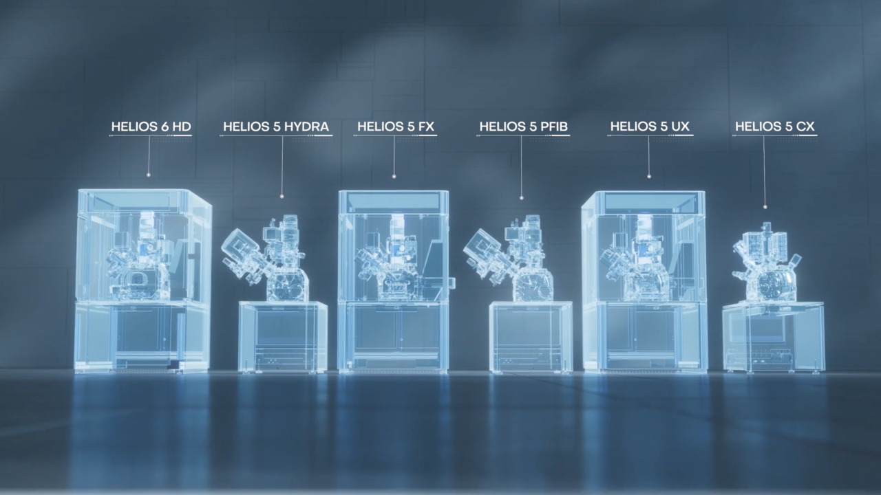
DualBeam Microscopes
Helios 5 PFIB DualBeam
Plasma focused ion beam scanning electron microscope for TEM sample preparation including 3D characterization, cross-sectioning and micromachining.
Join the Conversation
c7c8 - Key/Specs/Resources/Appl/Tech/Doc/Contact
Plasma focused ion beam instrument
Helios 5 Plasma FIB DualBeam FiB SEM Microscope
The Thermo Scientific Helios 5 Plasma FIB (PFIB) DualBeam (focused ion beam scanning electron microscope, or FIB-SEM) delivers unmatched capabilities for materials science and semiconductor applications. For materials science researchers, the Helios 5 PFIB DualBeam provides large-volume 3D characterization, gallium-free sample preparation, and precise micromachining. For manufacturers of semiconductor devices, advanced packaging technology, and display devices, the Helios 5 PFIB DualBeam delivers damage-free, large-area de-processing, fast sample preparation, and high-fidelity failure analysis.
Gallium-free STEM and TEM sample preparation
High-quality, gallium-free TEM and APT sample preparation thanks to the new PFIB column enabling 500 V Xe+ final polishing and delivering superior performance at all operating conditions.
Advanced automation
Fastest and easiest, automated, multisite in situ and ex situ TEM sample preparation and cross-sectioning using optional AutoTEM 5 Software.
Next-generation 2.5 μA xenon plasma FIB column
High throughput and quality statistically relevant 3D characterization, cross-sectioning and micromachining using next generation 2.5 μA Xenon Plasma FIB column (PFIB).
Multi-modal subsurface and 3D information
Access high-quality, multi-modal subsurface and 3D information with precise targeting of the region of interest using optional Auto Slice & View 4 (AS&V4) Software.
Sub-nanometer performance at low energies
Reveal the finest details using best-in-class Elstar Electron Column with high-current UC+ monochromator technology, enabling sub-nanometer performance at low energies.
Complete sample information
The most complete sample information with sharp, refined, and charge-free contrast obtained from up to six integrated in-column and below-the-lens detectors.
Advanced capabilities
Most advanced capabilities for electron and ion beam induced deposition and etching on FIB/SEM systems with optional Thermo Scientific MultiChem or GIS Gas Delivery Systems.
Artifact-free imaging
Artifact-free imaging based on integrated sample cleanliness management and dedicated imaging modes such as SmartScan™ and DCFI Modes.
Short time to nanoscale information
Shortest time to nanoscale information for users with any experience level with SmartAlign and FLASH technologies.
Precise sample navigation
Precise sample navigation tailored to individual application needs thanks to the high stability and accuracy of 150 mm Piezo stage and optional in-chamber Nav-Cam.
Semiconductor device deprocessing
The combination of Dx chemistry and the plasma FIB beam provides a unique, site-specific, deprocessing and failure analysis workflow for advanced logic, 3D NAND, and DRAM.
High-speed, large-area cross-sectioning
The next-generation 2.5 μA xenon PFIB column provides high-throughput, high-quality, statistically relevant 3D characterization, cross-sectioning, and micromachining.
TEM sample preparation
Perform high-quality, single layer planar and cross-sectional, top-down, and inverted TEM sample preparation by combining PFIB deprocessing and Thermo Scientific guided workflows.
Sub-nanometer, low-energy SEM performance
Reveal the finest details using the best-in-class Elstar Electron Column with high-current UC+ monochromator technology, enabling sub-nanometer performance at low energies.
Advanced automation
Carry out automated deprocessing with end pointing. SmartAlign and FLASH technologies make for a short time to nanoscale information for users with any experience level.
Complete sample information
Obtain the most complete sample information with sharp, refined, and charge-free contrast from up to six integrated in-column and below-the-lens detectors.
Artifact-free imaging
Obtain artifact-free imaging with in situ auto rocking polish and dedicated imaging modes such as SmartScan and DCFI modes.
Precise sample navigation
Experience precise sample navigation tailored to individual application needs from the flexible 5-axis motorized stage configuration and ultra-high-resolution stage options.
Style Sheet for Products Table Specifications
| Helios 5 PFIB CXe DualBeam | Helios 5 PFIB UXe DualBeam | |
| Electron optics |
| |
| Electron beam resolution |
| |
| Electron beam parameter space |
| |
| Ion optics |
| |
| Detectors |
| |
| Stage and sample | Flexible 5-axis motorized stage:
| High-precision, 5-axis motorized stage with XYR axis, piezo-driven
|
*Available as an option, configuration dependent
| Helios 5 PFIB CXe DualBeam | Helios 5 PFIB UXe DualBeam | Helios 5 PFIB HXe DualBeam | |
| Application | Advanced packaging and display R&D and failure analysis | Advanced memory failure analysis | Advanced logic failure analysis |
| Electron optics |
| ||
| Electron beam resolution |
| ||
| Ion optics |
| ||
| Stage and sample | Flexible 5-axis motorized stage:
| High-precision, 5-axis motorized stage with XYR axis, piezo-driven
| 5-axis, all-Piezo-driven UHR stage
|
Style Sheet for Komodo Tabs
Style Sheet to change H2 style to p with em-h2-header class
Style Sheet to change H3 to p with em-h3-header class
Style Sheet to change Applications H3 to p with em-h3-header class

Partnering in sustainability — ACT label
Understand your lab's environmental impact with the Helios 5 PFIB’s ACT label. Created by My Green Lab, the ACT label sets the standard for determining the environmental impact of laboratory products and helps labs make informed, sustainable purchasing decisions.

3D EBSD reconstruction of zircalloy sample (250 x 250 x 220 µm³) produced with he Helios G4 PFIB DualBeam, AS&V4 Software, and Thermo Scientific Avizo Software.

500 μm wide cross section for scratch testing and adhesion in
paint coatings.

Thermo Fisher Scientific PFA Demo Days
To support semiconductor manufacturing needs, Thermo Fisher Scientific continues to bring new capabilities to our industry-leading failure analysis, metrology and characterization solutions.
In our Thermo Fisher Scientific PFA Demo Days, we showcase our latest innovations for sample preparation and FinFET logic circuit delayering.
Advanced DualBeam automation for every need
Register for our exclusive webinar to learn how easy it has become to automate daily routine tasks on your DualBeam instrument using our Python-based AutoScript 4 API. Automation can also increase throughput, reproducibility and ease of use, quicken time to data and boost efficiency.
The Thermo Scientific Helios DualBeam
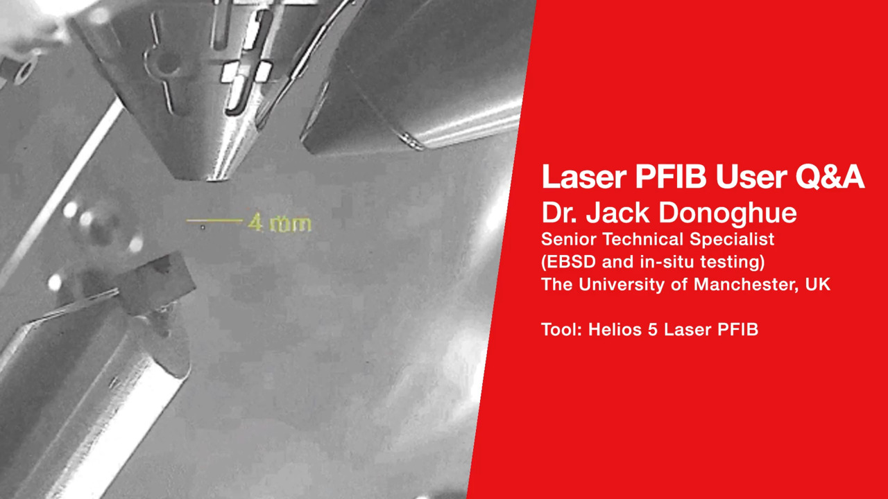
Interview - Laser PFIB use case from Manchester University
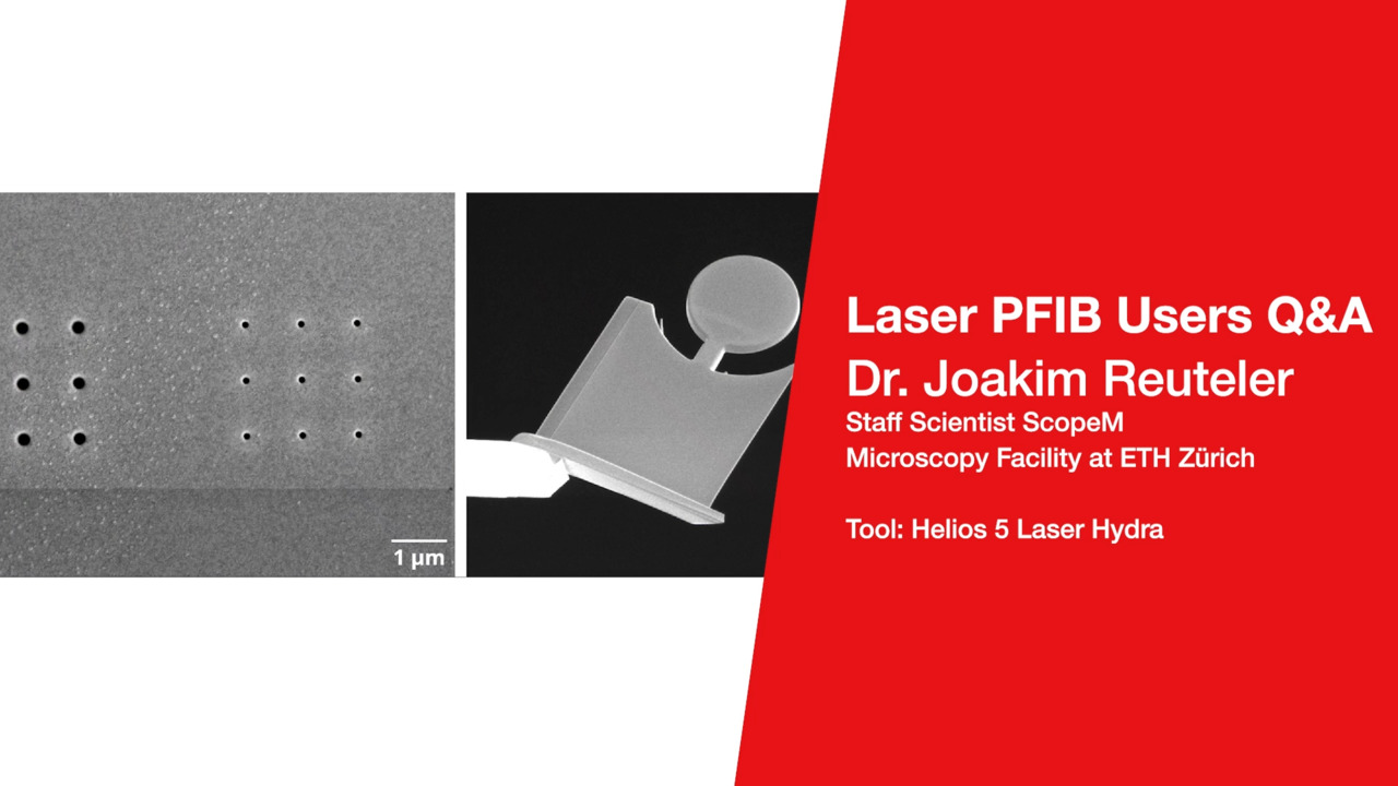
Interview - Laser PFIB use case from ScopeM
3D EBSD reconstruction of zircalloy sample (250 x 250 x 220 µm³) produced with he Helios G4 PFIB DualBeam, AS&V4 Software, and Thermo Scientific Avizo Software.
500 μm wide cross section for scratch testing and adhesion in
paint coatings.
Thermo Fisher Scientific PFA Demo Days
To support semiconductor manufacturing needs, Thermo Fisher Scientific continues to bring new capabilities to our industry-leading failure analysis, metrology and characterization solutions.
In our Thermo Fisher Scientific PFA Demo Days, we showcase our latest innovations for sample preparation and FinFET logic circuit delayering.
Advanced DualBeam automation for every need
Register for our exclusive webinar to learn how easy it has become to automate daily routine tasks on your DualBeam instrument using our Python-based AutoScript 4 API. Automation can also increase throughput, reproducibility and ease of use, quicken time to data and boost efficiency.
The Thermo Scientific Helios DualBeam
Interview - Laser PFIB use case from Manchester University
Interview - Laser PFIB use case from ScopeM

Fundamental Materials Research
Novel materials are investigated at increasingly smaller scales for maximum control of their physical and chemical properties. Electron microscopy provides researchers with key insight into a wide variety of material characteristics at the micro- to nano-scale.

Process control using electron microscopy
Modern industry demands high throughput with superior quality, a balance that is maintained through robust process control. SEM and TEM tools with dedicated automation software provide rapid, multi-scale information for process monitoring and improvement.

Quality control and failure analysis
Quality control and assurance are essential in modern industry. We offer a range of EM and spectroscopy tools for multi-scale and multi-modal analysis of defects, allowing you to make reliable and informed decisions for process control and improvement.

Semiconductor Advanced Packaging
Performance, power efficiency, area, and cost are driving packaging innovations. Learn how workflows provide fast, precise, and accurate time-to-data.

Semiconductor Failure Analysis
Complex semiconductor device structures result in more places for defects to hide. Learn more about failure analysis solutions to isolate, analyze, and repair defects.

Semiconductor materials characterization
Many factors impact yield, performance, and reliability. Learn more about solutions to characterize physical, structural, and chemical properties.

Semiconductor power devices
Novel architectures and materials pose new challenges. Learn how to pinpoint faults and characterize materials, structures, and interfaces.

Semiconductor research and development
Innovation starts with research and development. Learn more about solutions to help you understand innovative structures and materials at the atomic level.

Semiconductor display technology
Display technologies are evolving to improve display quality and light conversion efficiency. Learn how metrology, failure analysis, and characterization solutions provide insights.

(S)TEM Sample Preparation
DualBeam microscopes enable the preparation of high-quality, ultra-thin samples for (S)TEM analysis. Thanks to advanced automation, users with any experience level can obtain expert-level results for a wide range of materials.

APT Sample Preparation
Atom probe tomography (APT) provides atomic-resolution 3D compositional analysis of materials. Focused ion beam (FIB) microscopy is an essential technique for high-quality, orientation, and site-specific sample preparation for APT characterization.

In Situ experimentation
Direct, real-time observation of microstructural changes with electron microscopy is necessary to understand the underlying principles of dynamic processes such as recrystallization, grain growth, and phase transformation during heating, cooling, and wetting.

Multi-scale analysis
Novel materials must be analyzed at ever higher resolution while retaining the larger context of the sample. Multi-scale analysis allows for the correlation of various imaging tools and modalities such as X-ray microCT, DualBeam, Laser PFIB, SEM and TEM.

3D Materials Characterization
Development of materials often requires multi-scale 3D characterization. DualBeam instruments enable serial sectioning of large volumes and subsequent SEM imaging at nanometer scale, which can be processed into high-quality 3D reconstructions of the sample.

Cross-sectioning
Cross sectioning provides extra insight by revealing sub-surface information. DualBeam instruments feature superior focused ion beam columns for high-quality cross sectioning. With automation, unattended high-throughput processing of samples is possible.

Semiconductor Laser Ablation
Laser ablation provides high-throughput milling of semiconductor devices for imaging and analysis with electron microscopy, while still preserving sample integrity. Access large-volume 3D data and optimize milling conditions to best suit your sample type.

Nanoprobing
As device complexity increases, so does the number of places defects have to hide. Nanoprobing provides the precise localization of electrical faults, which is critical for an effective transmission electron microscopy failure analysis workflow.

Device Delayering
Shrinking feature size, along with advanced design and architecture, results in increasingly challenging failure analysis for semiconductors. Damage-free delayering of devices is a critical technique for the detection of buried electrical faults and failures.
(S)TEM Sample Preparation
DualBeam microscopes enable the preparation of high-quality, ultra-thin samples for (S)TEM analysis. Thanks to advanced automation, users with any experience level can obtain expert-level results for a wide range of materials.
APT Sample Preparation
Atom probe tomography (APT) provides atomic-resolution 3D compositional analysis of materials. Focused ion beam (FIB) microscopy is an essential technique for high-quality, orientation, and site-specific sample preparation for APT characterization.
In Situ experimentation
Direct, real-time observation of microstructural changes with electron microscopy is necessary to understand the underlying principles of dynamic processes such as recrystallization, grain growth, and phase transformation during heating, cooling, and wetting.
Multi-scale analysis
Novel materials must be analyzed at ever higher resolution while retaining the larger context of the sample. Multi-scale analysis allows for the correlation of various imaging tools and modalities such as X-ray microCT, DualBeam, Laser PFIB, SEM and TEM.
3D Materials Characterization
Development of materials often requires multi-scale 3D characterization. DualBeam instruments enable serial sectioning of large volumes and subsequent SEM imaging at nanometer scale, which can be processed into high-quality 3D reconstructions of the sample.
Cross-sectioning
Cross sectioning provides extra insight by revealing sub-surface information. DualBeam instruments feature superior focused ion beam columns for high-quality cross sectioning. With automation, unattended high-throughput processing of samples is possible.
Semiconductor Laser Ablation
Laser ablation provides high-throughput milling of semiconductor devices for imaging and analysis with electron microscopy, while still preserving sample integrity. Access large-volume 3D data and optimize milling conditions to best suit your sample type.
Nanoprobing
As device complexity increases, so does the number of places defects have to hide. Nanoprobing provides the precise localization of electrical faults, which is critical for an effective transmission electron microscopy failure analysis workflow.
Device Delayering
Shrinking feature size, along with advanced design and architecture, results in increasingly challenging failure analysis for semiconductors. Damage-free delayering of devices is a critical technique for the detection of buried electrical faults and failures.
Electron microscopy services
To ensure optimal system performance, we provide you access to a world-class network of field service experts, technical support, and certified spare parts.
Electron microscopy support and resources
Style Sheet for Support and Service footer
Style Sheet for Fonts
Style Sheet for Cards