Search Thermo Fisher Scientific

c7c8 - Key/Specs/Resources/Appl/Tech/Doc/Contact
Materials characterization
Advanced materials characterization labs require access to the latest techniques and will push analytical tools, including SEMs, to the extremes of their capabilities. Most of these labs are multi-user facilities that accommodate users with varying degrees of experience. Time on the microscope is precious, and excessive time spent on maintenance, alignments, training, or image optimization needs to be avoided.
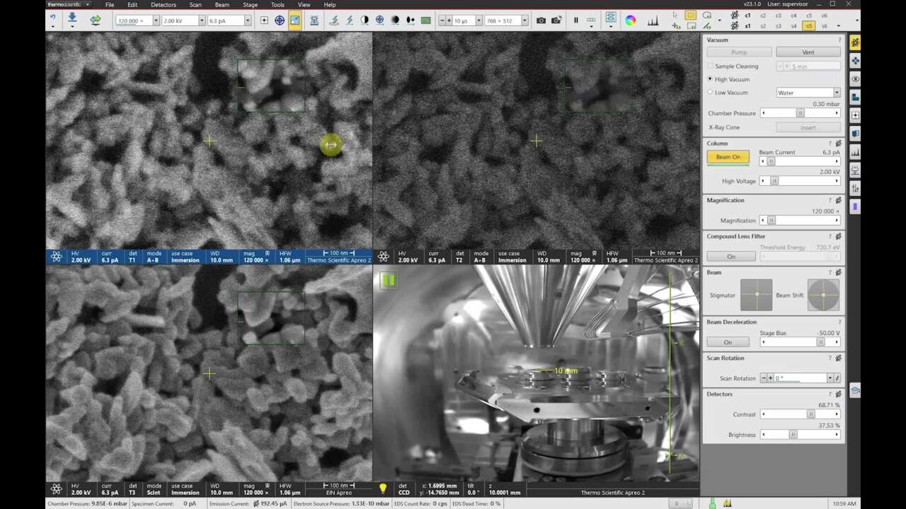
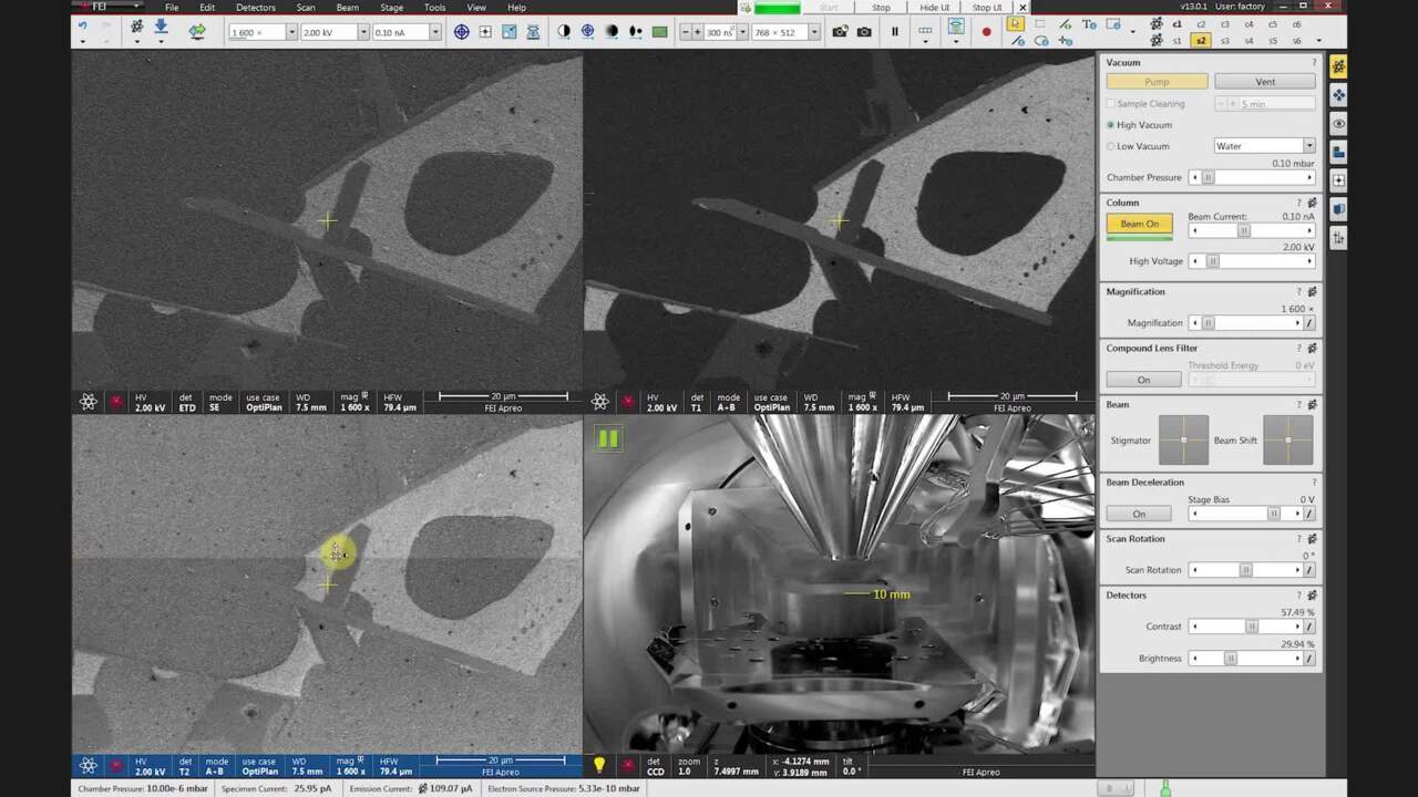
Apreo 2 Scanning Electron Microscope
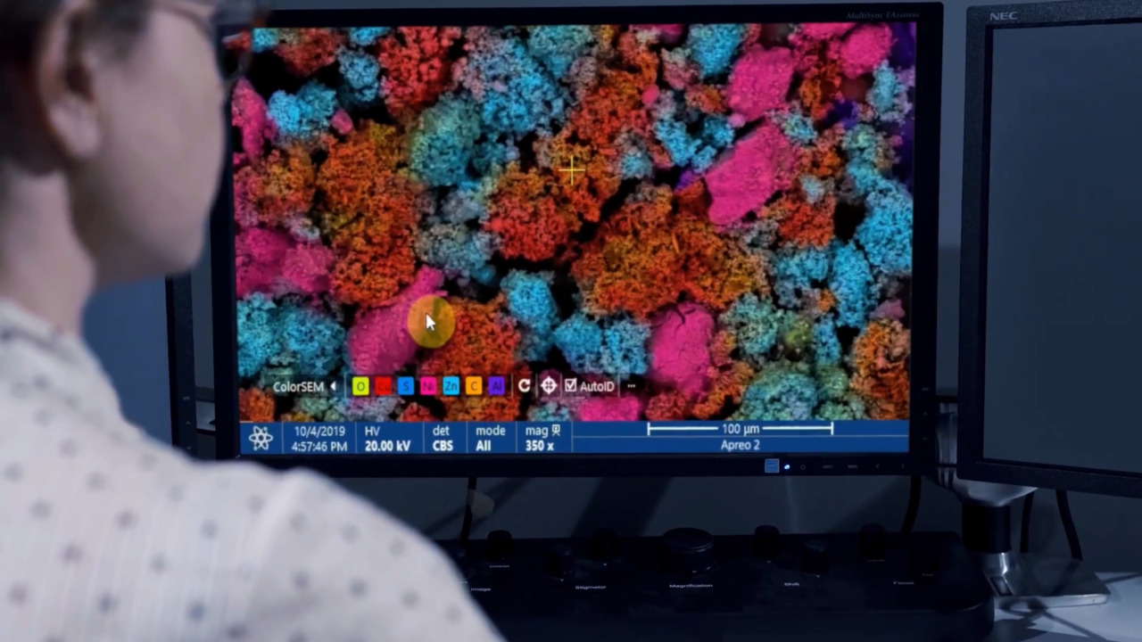
The new Thermo Scientific Apreo 2 SEM expands access to high-performance imaging and analytics to all levels of microscopy expertise. With Thermo Scientific ChemiSEM Technology, a unique live elemental imaging capability, compositional information is always available, through the most intuitive interface. Eliminating all the hassle associated with typical EDS implementations, ChemiSEM Technology offers unprecedented time to result and ease of use.
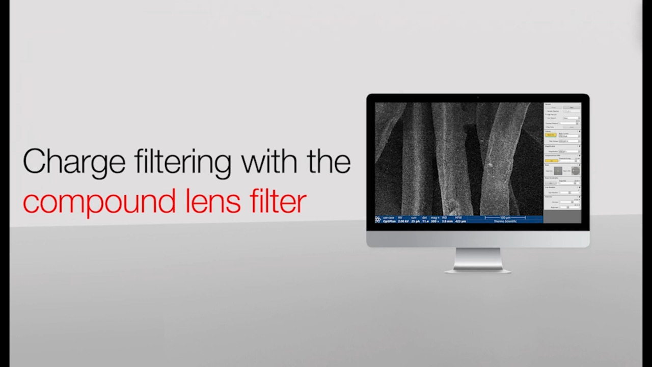
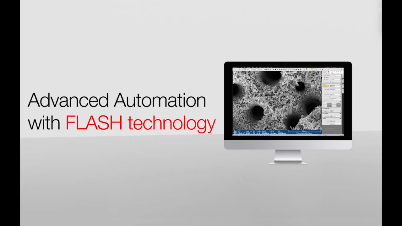
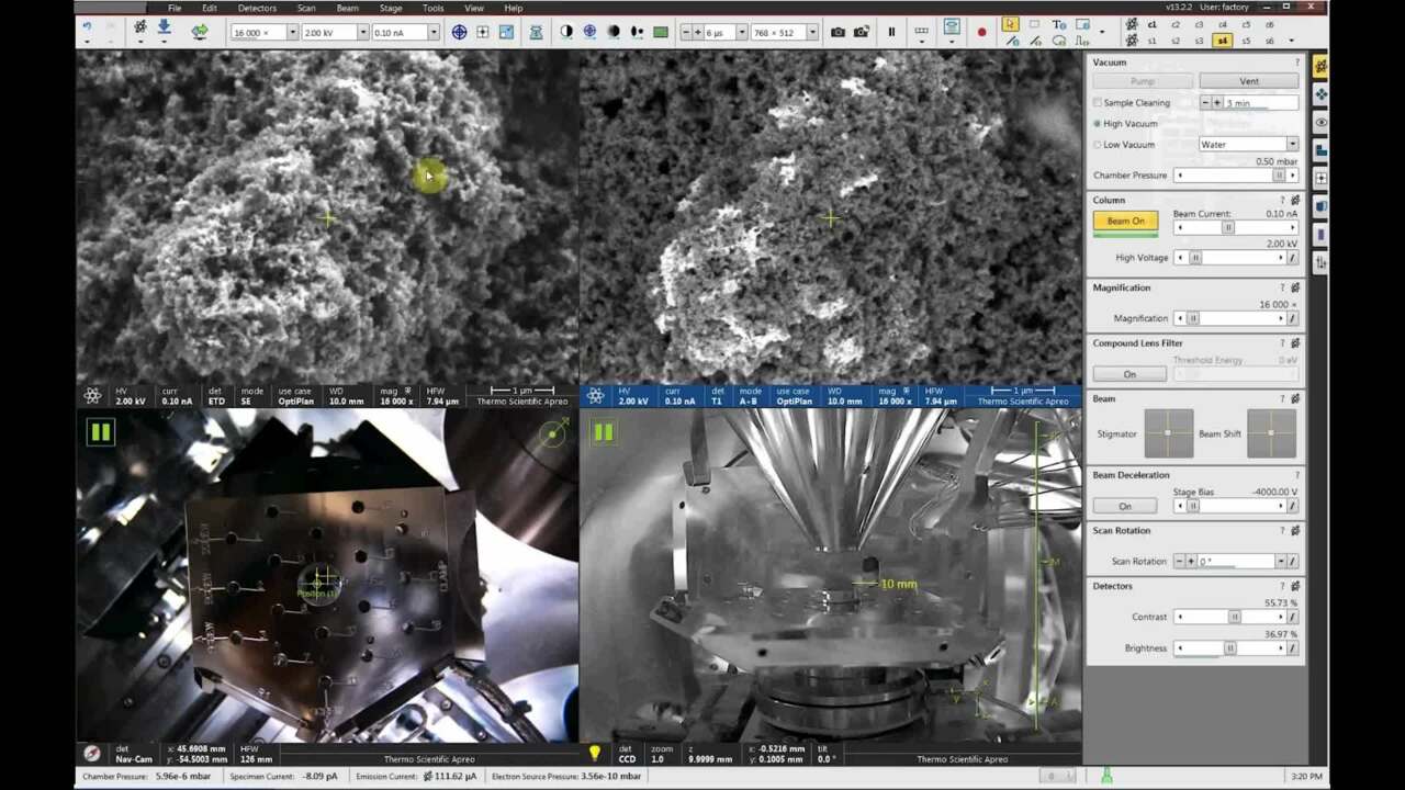
The Apreo 2 SEM poses much smaller demands on users and lab managers with Thermo Scientific SmartAlign Technology, an optics system that aligns itself. Furthermore, the Apreo 2 SEM automates the image fine-tuning process with Thermo Scientific FLASH technology. FLASH Technology executes any necessary corrections to lens centering, the stigmators, and final focus of the image. The combination of these technologies means that users new to electron microscopy can access the high-end performance of the Apreo 2 SEM. Additionally, the Apreo 2 SEM is the only SEM with a 1-nanometer resolution at 10 mm analytical working distance. No longer does long working distance mean poor imaging. With the Apreo 2 SEM, anyone will be able to confidently get great results.
Apreo 2 SEM video teaser
High performance, resolution, and contrast
The combination of advanced optics, detection and automation in Apreo 2 makes obtaining high resolution imaging possible even for users new to SEM.

Wide range of sample types
Apreo 2 was designed for maximum flexibility. High quality, high resolution imaging is possible regardless of target samples properties. Insulators, beam sensitive or magnetic materials can all be imaged with ease thanks to Apreo 2's unique optics, detection and beam control options.

Click image to enlarge
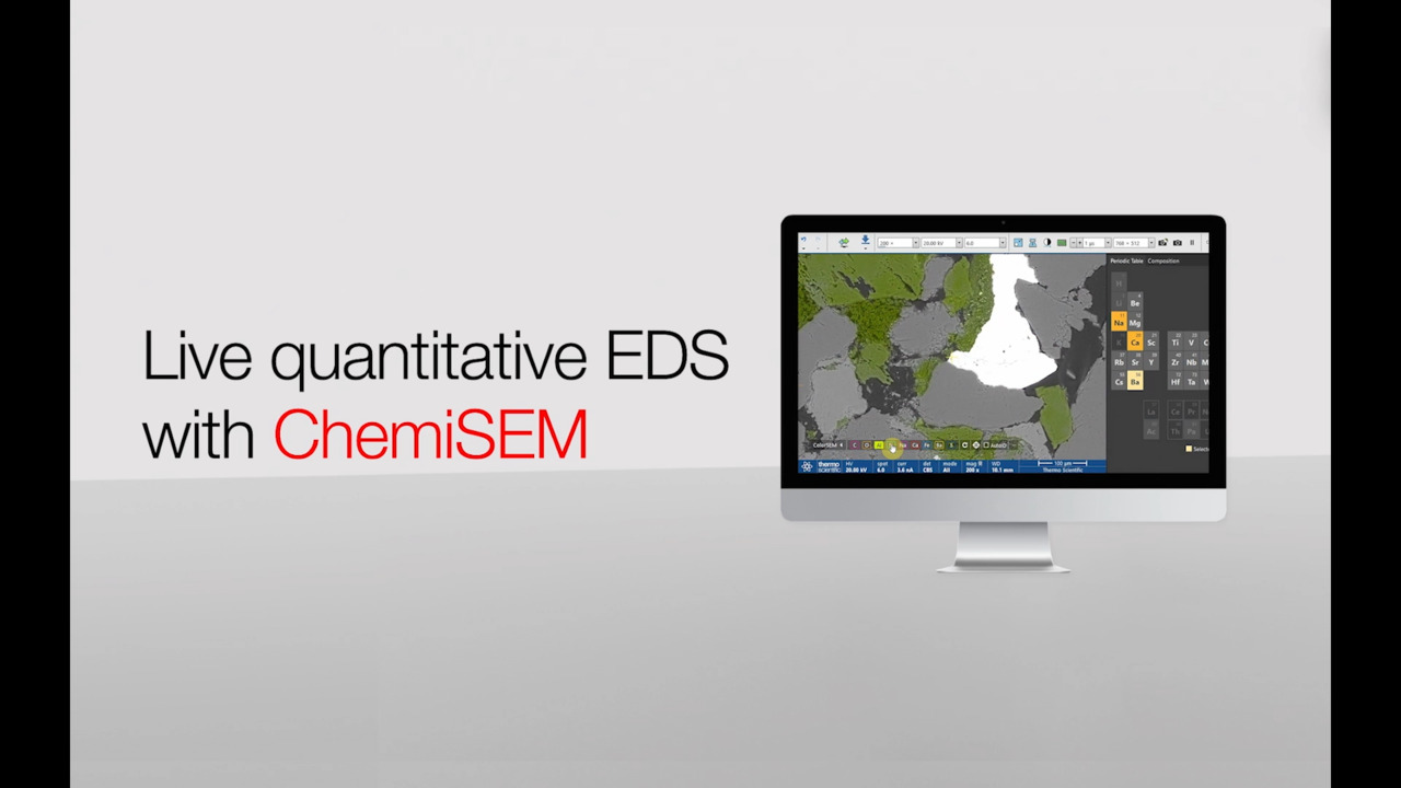
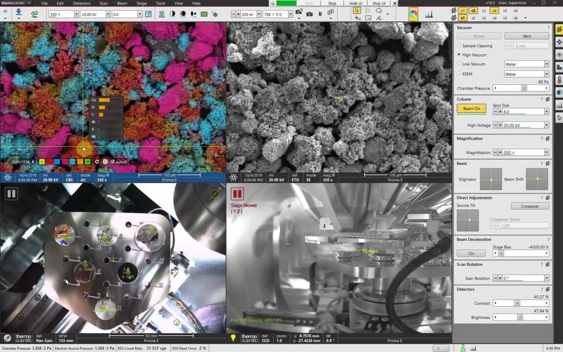
Live quantitative EDS with ChemiSEM
Elemental information at your fingertips with ChemiSEM, which provides live quantitative elemental mapping for unprecedented time to result and ease of use.
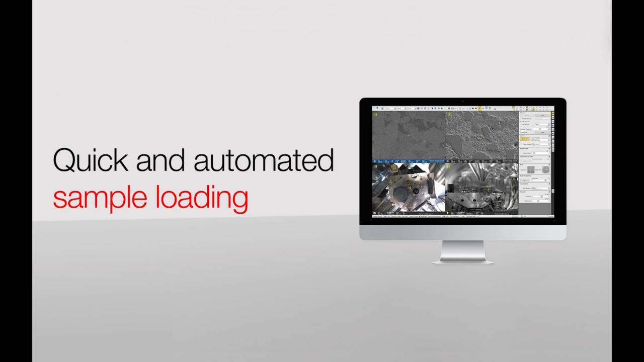
Quick and easy sample loading
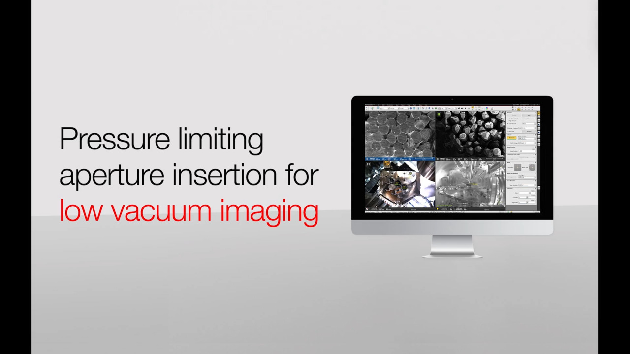
Easy access to the stage, a convenient multi-sample holder, and a fast pump down ensures no time is wasted loading samples. An automated routine to insert and remove a pressure limiting aperture (PLA) allows for a seamless switch between high and low vacuum without opening the chamber.
Advanced automation
From optics, to image acquisition, Apreo 2 provides a range of automated features to make imaging time as effective and efficient as possible. Flash Technology automates image fine tuning The unique Undo function permits efficient exploration of imaging conditions Thermo Scientific Maps software automates large area acquisition with up to 4 different simultaneous signals

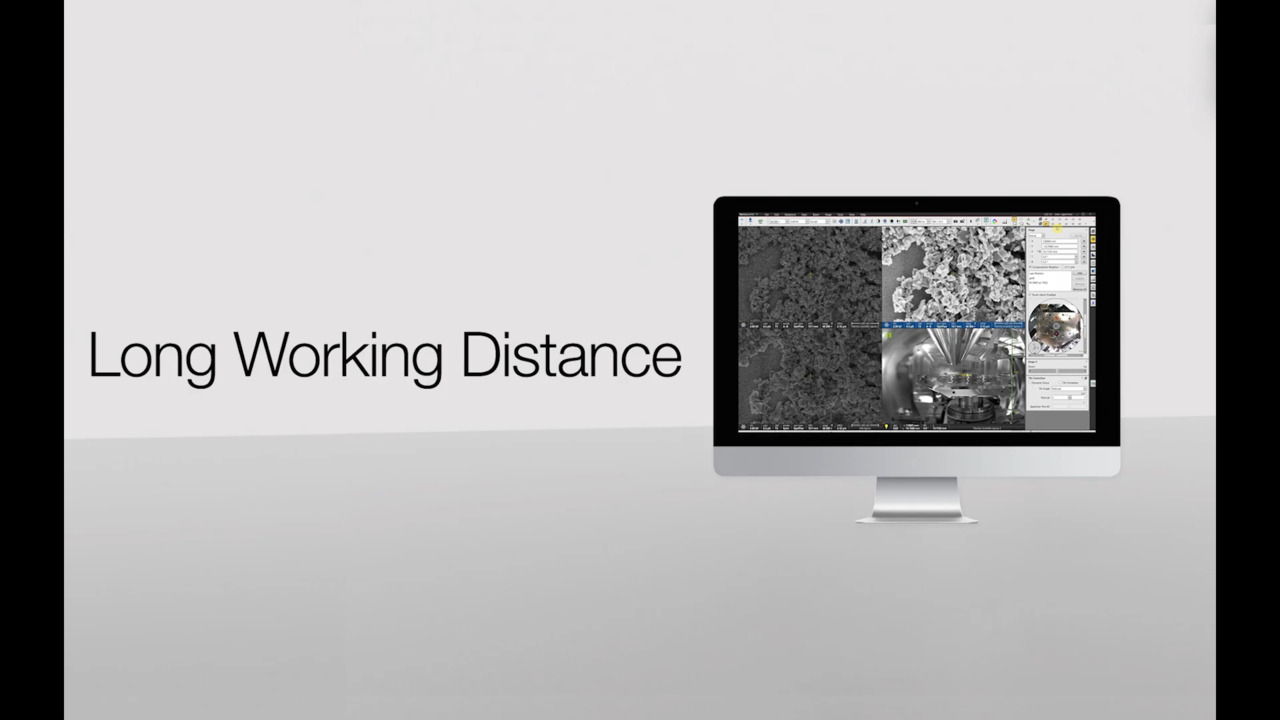
Performance at long working distance
Apreo 2 is the only SEM that offers high-resolution performance (1nm) and excellent image quality at analytical working distance (10mm). Sample morphology, topography and surface information can all be simultaneously explored while being at a safe distance from the pole piece. Thanks to its high-speed and high-sensitivity in-lens backscattered detector, BSE are still detected even at extremely low beam currents (as low as few pA).
Style Sheet for Products Table Specifications
Apreo 2 S | Apreo 2 C | |
Resolution |
|
|
Standard detectors |
|
|
PivotBeam |
|
|
Optional detectors |
| |
ChemiSEM Technology (optional) |
| |
Landing energy range |
| |
Stage bias (beam deceleration) |
| |
Low vacuum mode |
| |
Stage |
| |
Maximum beam current |
| |
Standard sample holder |
| |
Chamber |
| |
Style Sheet to change H2 style to p with em-h2-header class
Style Sheet for Komodo Tabs
Long working distance imaging on palladium nanoparticles on cerium oxide matrix.
Easy nanoparticles imaging at 10 mm working distance.
Highlight contrast that would otherwise go unnoticed

High material contrast and easy platinum nanoparticles imaging at 10 mm working.
This video demonstrates how Apreo's Trinity detection system quickly answers all our questions about a sample.
On-demand webinar: Introduction to Apreo 2 - Unmatched versatility powered by ChemiSEM Technology
This is an introduction on-demand webinar to be followed by a more extensive overview of the Apreo 2 SEM, its features, functionalities, ChemiSEM technology, and a demonstration of the Apreo 2 in action. Attend this on-demand webinar to:
- Learn about the latest in analytical UHR-SEM from Thermo Fisher Scientific.
- Get introduced to the Apreo 2 SEM.
Webinar: Scanning electron microscopy: selecting the right technology for your needs
This on-demand webinar has been designed to help you decide which SEM best meets your unique needs. We present an overview of Thermo Fisher Scientific SEM technology for multi-user research labs and focus on how these wide-ranging solutions deliver performance, versatility, in situ dynamics and faster time to results. Watch this webinar if you are interested in:
- How the needs for different microanalysis modalities are met (EDX, EBSD, WDS, CL, etc.).
- How samples are characterized in their natural state without the need for sample preparation.
- How new advanced automation allows researchers to save time and increase productivity.

Ag particles on silica

Palladium nanoparticles imaged with ChemiSEM. Frame time: 30 seconds.

Lithium ion cathode precursor

A silver-copper mix imaged on Apreo 2 with ChemiSEM technology in less than a minute and a half.

Au/Pd nanoparticle on TiO2 support. Within a 1-minute frame time, ChemiSEM technology maps the composition, even on nanoparticle feature sizes.

Blend of polystyrene and polyacrylic acid polymers

Semiconductor bond wire taken on Apreo at 1kV.

Semiconductor bond wire taken on Apreo at 2kV, Mix detector.

Semiconductor bond wire taken on Apreo at 5kV, LVD detector.

Semiconductor bond wire in mod compound taken on Apreo at 1kV.

Aluminum Tin alloy after heating

Ceramic heating stage imaged with ChemiSEM Technology

Dental amalgam imaged with ChemiSEM Technology. The dental amalgam is a filler rich in mercury and a metal alloy mixture of silver, tin and copper.

Diatoms

Gold nanocubes

Gold palladium particle on titania

Iron Oxide

Mushroom Spores

Nanoporous gold

Pollen

Polymer battery separator

Rene N5 superalloy for turbine blades. Cross section of a thermally cycled part showing the presence of oxide intrusions from the surface

Silicon graphite battery anode imaged with ChemiSEM Technology. The image shows the distribution of the silicon and carbon in the area of interest and highlight the presence of a nickel-rich contaminant.

ChemiSEM image of a cross section of an electrode active material showing the presence of zirconium-rich impurities and the distribution of the fluorine-rich binder.

Calcium carbonate particles (rod-like polymorph) imaged with an acceleration voltage of 1 keV

Calcium carbonate particles (spindle-like polymorph) imaged with an acceleration voltage of 500 V using beam deceleration

Bright field (BF) STEM image of bamboo-like carbon nanotubes with iron nanoparticles

Bright field (BF) and high angle annular dark field (HAADF) STEM images of MikNo zinc oxide platelets

MicNo® ZnO platelets (Entekno Materials) made of zinc oxide nanoparticles. Images have been taken with an acceleration voltage of 1 keV
Long working distance imaging on palladium nanoparticles on cerium oxide matrix.
Easy nanoparticles imaging at 10 mm working distance.
Highlight contrast that would otherwise go unnoticed
High material contrast and easy platinum nanoparticles imaging at 10 mm working.
This video demonstrates how Apreo's Trinity detection system quickly answers all our questions about a sample.
On-demand webinar: Introduction to Apreo 2 - Unmatched versatility powered by ChemiSEM Technology
This is an introduction on-demand webinar to be followed by a more extensive overview of the Apreo 2 SEM, its features, functionalities, ChemiSEM technology, and a demonstration of the Apreo 2 in action. Attend this on-demand webinar to:
- Learn about the latest in analytical UHR-SEM from Thermo Fisher Scientific.
- Get introduced to the Apreo 2 SEM.
Webinar: Scanning electron microscopy: selecting the right technology for your needs
This on-demand webinar has been designed to help you decide which SEM best meets your unique needs. We present an overview of Thermo Fisher Scientific SEM technology for multi-user research labs and focus on how these wide-ranging solutions deliver performance, versatility, in situ dynamics and faster time to results. Watch this webinar if you are interested in:
- How the needs for different microanalysis modalities are met (EDX, EBSD, WDS, CL, etc.).
- How samples are characterized in their natural state without the need for sample preparation.
- How new advanced automation allows researchers to save time and increase productivity.
Ag particles on silica
Palladium nanoparticles imaged with ChemiSEM. Frame time: 30 seconds.
Lithium ion cathode precursor
A silver-copper mix imaged on Apreo 2 with ChemiSEM technology in less than a minute and a half.
Au/Pd nanoparticle on TiO2 support. Within a 1-minute frame time, ChemiSEM technology maps the composition, even on nanoparticle feature sizes.
Blend of polystyrene and polyacrylic acid polymers
Semiconductor bond wire taken on Apreo at 1kV.
Semiconductor bond wire taken on Apreo at 2kV, Mix detector.
Semiconductor bond wire taken on Apreo at 5kV, LVD detector.
Semiconductor bond wire in mod compound taken on Apreo at 1kV.
Aluminum Tin alloy after heating
Ceramic heating stage imaged with ChemiSEM Technology
Dental amalgam imaged with ChemiSEM Technology. The dental amalgam is a filler rich in mercury and a metal alloy mixture of silver, tin and copper.
Diatoms
Gold nanocubes
Gold palladium particle on titania
Iron Oxide
Mushroom Spores
Nanoporous gold
Pollen
Polymer battery separator
Rene N5 superalloy for turbine blades. Cross section of a thermally cycled part showing the presence of oxide intrusions from the surface
Silicon graphite battery anode imaged with ChemiSEM Technology. The image shows the distribution of the silicon and carbon in the area of interest and highlight the presence of a nickel-rich contaminant.
ChemiSEM image of a cross section of an electrode active material showing the presence of zirconium-rich impurities and the distribution of the fluorine-rich binder.
Calcium carbonate particles (rod-like polymorph) imaged with an acceleration voltage of 1 keV
Calcium carbonate particles (spindle-like polymorph) imaged with an acceleration voltage of 500 V using beam deceleration
Bright field (BF) STEM image of bamboo-like carbon nanotubes with iron nanoparticles
Bright field (BF) and high angle annular dark field (HAADF) STEM images of MikNo zinc oxide platelets
MicNo® ZnO platelets (Entekno Materials) made of zinc oxide nanoparticles. Images have been taken with an acceleration voltage of 1 keV

Fundamental Materials Research
Novel materials are investigated at increasingly smaller scales for maximum control of their physical and chemical properties. Electron microscopy provides researchers with key insight into a wide variety of material characteristics at the micro- to nano-scale.

Quality control and failure analysis
Quality control and assurance are essential in modern industry. We offer a range of EM and spectroscopy tools for multi-scale and multi-modal analysis of defects, allowing you to make reliable and informed decisions for process control and improvement.

Semiconductor research and development
Innovation starts with research and development. Learn more about solutions to help you understand innovative structures and materials at the atomic level.

Semiconductor metrology
Manufacturing today’s complex semiconductors requires exact process controls. Learn more about advanced metrology and analysis solutions to accelerate yield learnings.

Semiconductor Failure Analysis
Complex semiconductor device structures result in more places for defects to hide. Learn more about failure analysis solutions to isolate, analyze, and repair defects.

Semiconductor materials characterization
Many factors impact yield, performance, and reliability. Learn more about solutions to characterize physical, structural, and chemical properties.

Semiconductor display technology
Display technologies are evolving to improve display quality and light conversion efficiency. Learn how metrology, failure analysis, and characterization solutions provide insights.

EDS Analysis with ChemiSEM Technology
Energy dispersive X-ray spectroscopy for materials characterization.

Energy Dispersive Spectroscopy
Energy dispersive spectroscopy (EDS) collects detailed elemental information along with electron microscopy images, providing critical compositional context for EM observations. With EDS, chemical composition can be determined from quick, holistic surface scans down to individual atoms.

Imaging Hot Samples
Studying materials in real-world conditions often involves working at high temperatures. The behavior of materials as they recrystallize, melt, deform, or react in the presence of heat can be studied in situ with scanning electron microscopy or DualBeam tools.

Cathodoluminescence
Cathodoluminescence (CL) describes the emission of light from a material when it is excited by an electron beam. This signal, captured by a specialized CL detector, carries information on the sample’s composition, crystal defects, or photonic properties.

Multi-scale analysis
Novel materials must be analyzed at ever higher resolution while retaining the larger context of the sample. Multi-scale analysis allows for the correlation of various imaging tools and modalities such as X-ray microCT, DualBeam, Laser PFIB, SEM and TEM.

Semiconductor Analysis and Imaging
Thermo Fisher Scientific offers scanning electron microscopes for every function of a semiconductor lab, from general imaging tasks to advanced failure analysis techniques requiring precise voltage-contrast measurements.
EDS Analysis with ChemiSEM Technology
Energy dispersive X-ray spectroscopy for materials characterization.
Energy Dispersive Spectroscopy
Energy dispersive spectroscopy (EDS) collects detailed elemental information along with electron microscopy images, providing critical compositional context for EM observations. With EDS, chemical composition can be determined from quick, holistic surface scans down to individual atoms.
Imaging Hot Samples
Studying materials in real-world conditions often involves working at high temperatures. The behavior of materials as they recrystallize, melt, deform, or react in the presence of heat can be studied in situ with scanning electron microscopy or DualBeam tools.
Cathodoluminescence
Cathodoluminescence (CL) describes the emission of light from a material when it is excited by an electron beam. This signal, captured by a specialized CL detector, carries information on the sample’s composition, crystal defects, or photonic properties.
Multi-scale analysis
Novel materials must be analyzed at ever higher resolution while retaining the larger context of the sample. Multi-scale analysis allows for the correlation of various imaging tools and modalities such as X-ray microCT, DualBeam, Laser PFIB, SEM and TEM.
Semiconductor Analysis and Imaging
Thermo Fisher Scientific offers scanning electron microscopes for every function of a semiconductor lab, from general imaging tasks to advanced failure analysis techniques requiring precise voltage-contrast measurements.
Electron microscopy services
To ensure optimal system performance, we provide you access to a world-class network of field service experts, technical support, and certified spare parts.
Electron microscopy support and resources
Style Sheet for Support and Service footer
Style Sheet for Fonts
Style Sheet for Cards