Search Thermo Fisher Scientific

DualBeam FIB-SEM Microscopes
Helios 5 EXL DualBeam
FIB-SEM TEM sample preparation for the semiconductor industry, enabling full-wafer analysis.
c7c8 - Key/Specs/Resources/Appl/Tech/Doc/Contact
Demand for high-performance, energy-efficient electronics is driving the development of advanced devices with ever smaller, more densely packed features and complex 3D structures. Ramping production of these cutting-edge microprocessors, memory devices, and other products is extremely challenging and requires high-resolution, atomic-scale analysis of features buried deep within the device. Transmission electron microscopy (TEM) is increasingly becoming the go-to technique for this kind of analysis and relies on high-quality samples produced with focused ion beam (FIB) milling.
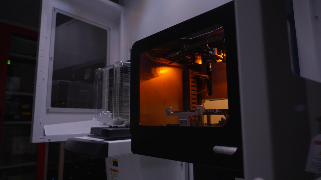
The Thermo Scientific Helios 5 EXL DualBeam is a 300mm full-wafer focused ion beam scanning electron microscope (FIB-SEM), designed to address TEM sample preparation challenges in the semiconductor industry. The Helios 5 EXL DualBeam is capable of preparing samples for today’s most advanced process nodes, including sub-5nm and gate-all-around technology.
Maximizing sample throughput and productivity
Utilizing advanced machine learning and closed-loop end pointing, the Helios 5 EXL DualBeam delivers enhanced cut placement precision and enables you to consistently extract high-quality lamella from your most challenging samples.
Flexible automation capabilities make ultra-thin TEM sample generation routine and consistent, providing unparalleled, sub-nanometer insight into more interfaces, films, and profiles to measure at sub-nanometer resolution. The Helios 5 EXL DualBeam ensures efficient and consistent TEM sample preparation workflows by combining wafer and defect navigation with recipe definition and execution in a single, fully integrated program. This automation supports a higher tool-to-operator ratio, maximizing sample throughput and technical resource productivity.
Revolutionizing Semiconductor Analysis: Thermo Scientific Helios 5 EXL Overview

TEM image of a Si/SiGe gate-all-around (GAA) fin.

TEM image of a gate cross-section along a nanowire.
Automated TEM sample preparation software
Thermo Scientific AutoTEM 5 Software combines wafer and defect navigation with recipe definition and execution in a single, fully integrated program, ensuring efficiency and consistency among operators with varying levels of expertise. AutoTEM Software simplifies TEM sample preparation, allowing users to easily schedule multi-site jobs for inverted, plan-view, and top-down TEM sample preparation workflows.
Repeatable, automated deposition and etch
Developed specifically to support automated TEM preparation, the Thermo Scientific MultiChem Gas Delivery System provides highly consistent deposition and etching capabilities and can be utilized with automated applications. The motorized injection needle with saved position presets can be accurately positioned for optimized, reproducible gas delivery to the sample surface. The MultiChem Gas Delivery System is also engineered for serviceability, maximizing tool uptime.
Precision FIB milling for advanced sample preparation
The Helios 5 EXL DualBeam includes the Thermo Scientific Phoenix Ion Column, which provides revolutionary low-kV performance and leading-edge TEM sample preparation.
Automated alignments, high resolution, and consistent results
The high-performance Thermo Scientific Elstar Electron Column features our unique UC monochromatic technology, offering improved resolution and TEM sample end-pointing. New SEM auto-alignments ensure consistent results across multiple tools and operators.
Automated sample manipulation and lift out
With an intuitive method for lift-out and transfer of TEM samples to a grid, the Thermo Scientific EasyLift Nanomanipulator offers low-drift, high-precision movements for simple and consistent creation of traditional or ultra-thin TEM lamella. Highly accurate, easy-to-use, and fast motorized rotation makes the EasyLift Nanomanipulator ideally suited for high-speed inverted or plan-view sample preparation.
Fab-compatible Automated FOUP Loader (AFL) option
The optional Automated FOUP Loader (AFL) enables the Helios 5 EXL DualBeam to be located inside the semiconductor wafer fab. By being closer to the wafer process line (near-line), it can deliver critical information up to three times faster than laboratory-based analysis of cleaved wafer pieces, accelerating the development of new processes and the yield ramp to high-volume production.
| Thermo Scientific Phoenix Ion Column |
|
| Thermo Scientific Elstar Electron Column |
|
| Gas delivery |
|
| Detectors |
|
| Sample handling |
|
| Additional options |
|
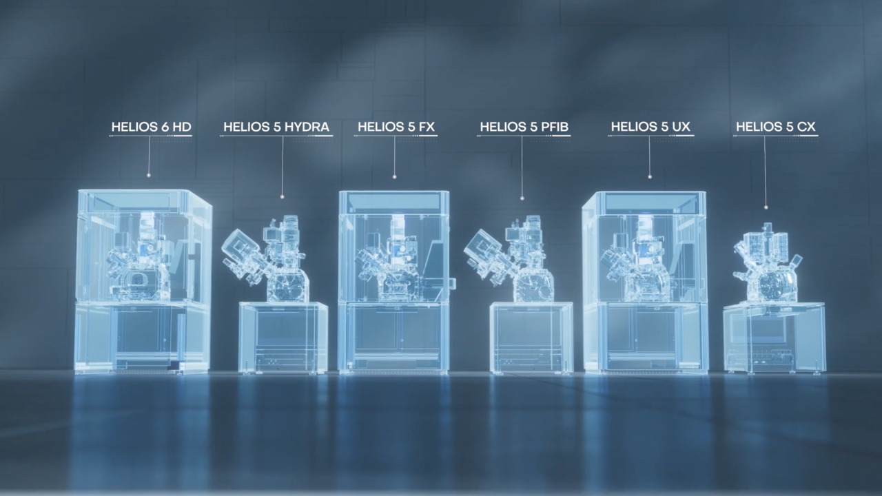
The Thermo Scientific Helios DualBeam Family
The Thermo Scientific Helios DualBeam Family

Semiconductor Advanced Packaging
Performance, power efficiency, area, and cost are driving packaging innovations. Learn how workflows provide fast, precise, and accurate time-to-data.

Semiconductor research and development
Innovation starts with research and development. Learn more about solutions to help you understand innovative structures and materials at the atomic level.

Semiconductor metrology
Manufacturing today’s complex semiconductors requires exact process controls. Learn more about advanced metrology and analysis solutions to accelerate yield learnings.

Semiconductor Failure Analysis
Complex semiconductor device structures result in more places for defects to hide. Learn more about failure analysis solutions to isolate, analyze, and repair defects.

Semiconductor materials characterization
Many factors impact yield, performance, and reliability. Learn more about solutions to characterize physical, structural, and chemical properties.

Semiconductor TEM Imaging and Analysis
Thermo Scientific transmission electron microscopes offer high-resolution imaging and analysis of semiconductor devices, enabling manufacturers to calibrate toolsets, diagnose failure mechanisms, and optimize overall process yields.

TEM Metrology
Advanced and automated TEM metrology routines deliver significantly greater precision than manual methods. This allows users to generate large amounts of statistically relevant data, with sub-angstrom-level specificity, that is free of operator bias.

Sample Preparation of Semiconductor Devices
Thermo Scientific DualBeam systems provide accurate TEM sample preparation for atomic-scale analysis of semiconductor devices. Automation and advanced machine learning technologies produce high-quality samples, at the correct location, and a low cost per sample.
Semiconductor TEM Imaging and Analysis
Thermo Scientific transmission electron microscopes offer high-resolution imaging and analysis of semiconductor devices, enabling manufacturers to calibrate toolsets, diagnose failure mechanisms, and optimize overall process yields.
TEM Metrology
Advanced and automated TEM metrology routines deliver significantly greater precision than manual methods. This allows users to generate large amounts of statistically relevant data, with sub-angstrom-level specificity, that is free of operator bias.
Sample Preparation of Semiconductor Devices
Thermo Scientific DualBeam systems provide accurate TEM sample preparation for atomic-scale analysis of semiconductor devices. Automation and advanced machine learning technologies produce high-quality samples, at the correct location, and a low cost per sample.
Electron microscopy services for
semiconductors
To ensure optimal system performance, we provide you access to a world-class network of field service experts, technical support, and certified spare parts.
Electron microscopy support and resources
Style Sheet to change Applications H3 to p with em-h3-header class
Style Sheet to change H3 to p with em-h3-header class
Style Sheet to change H2 style to p with em-h2-header class
Style Sheet for Komodo Tabs
Style Sheet for Support and Service footer
Style Sheet for Fonts
Style Sheet for Cards