Search Thermo Fisher Scientific

Materials Science
Hot Stage Microscopy
An SEM heating stage offers high quality in situ imaging and analysis at high temperatures.
Join the conversation
48ab - Appl/Samples/Products/Resources/Contact
Hot stage microscopy
Real-world materials applications often take place under variable environmental conditions, including high temperatures. The behavior of your heated material as it recrystallizes, melts, and deforms can inform critical macro- and microscopic observations, such as how a manufactured part might respond to stress or how feed materials behave during production. As a sample’s response to heat is a dynamic process, it must be paired with dynamic observation for accurate insight. Modern heating stages in electron microscopes allow for in situ experiments for high-resolution observation of heated materials. These demanding experiments are capable of linking sample morphology, environment, and thermodynamics, and can help you control the corresponding behavior of the bulk material.
SEM heating stages
There are many considerations when operating electron microscopes at elevated temperatures, such as the desired temperature range, sample size, and chemical environment. The following table shows what is possible with Thermo Scientific temperature stages.
Style Sheet for Products Table Specifications
Name | Application | Temperature | Max. Sample Size | Environment |
High vacuum heating stage | General-purpose heating, high resolution imaging, in-column detection, fast processes, electron-backscatter diffraction (EBSD) | Up to 1100°C (EBSD up to 900°C) | 10 mm | High vacuum |
Environmental SEM (ESEM) stage | Heating in gaseous environment: oxidation or other chemical reactions | Up to 1000°C or 1400°C, depending on the model | 5 mm | ESEM |
µHeater | Powder heating, chunk lift-out studies (DualBeam), STEM imaging, high-temperature EBSD and EDS, ramp rate of 10,000°C/s | Up to 1200°C | 50 µm | Any |
Cooling stage, WetSTEM | Precise control over humidity, wetting studies, modest heating | -20°C to +60°C | 3 mm | ESEM |

Gold on a silicon substrate at approximately 1080°C. The High Vacuum Heating Stage allows all in-lens detectors and imaging modes to be used to image the sample with excellent resolution and contrast.


Mixture of magnetite and hematite nanoparticles heated at 1030 °C.
Backscattered electron image (left) and EDS maps of iron and oxygen (right) acquired simultaneously.


Texture development on implant material. As the temperature increases from 700 °C to 1300 °C
we can observe a completely different surface structure. Pressure: 120 Pa.
 heated with a SEM hot stage.")
 heated with a SEM hot stage.")
Two-phase Co-Sb alloy during heating to 700°C on the High Vacuum Heating Stage. The antimony-rich
phase sublimated during heating, causing exposure of the second phase.
 Hydrophobic paper
Surface of hydrophobic treated paper - water condensation appears as droplets on top of the paper, rather than wetting the fibers. This experiment was carried out by controlling chamber pressure and stage temperature in a Quattro ESEM.
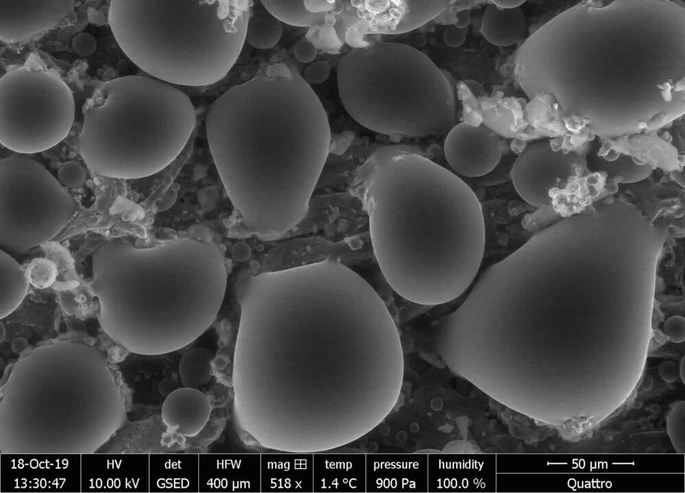
 Expancel
Akzo Nobel Expancel Microspheres, a filler material that expands with increased temperature, is observed in situ using an ESEM heating stage. Working at elevated chamber pressure allows the system to deal with any outgassing that is produced.
 Super-absorption
Sodium polyacrylate is a super-absorbent polymer with broad application in consumer products. Here, humidity is introduced into the SEM chamber and swelling of the material is observed in situ.
 Melting solder
The wetting behavior of solder droplets is studied in situ using an ESEM heating stage.
 Melting of 70% chocolate
Melting of 70% chocolate, under precisely controlled temperature and humidity conditions.
 Freezing tomato
Freezing can affect food structure, such as this tomato surface. Using a cooling stage, formation and sublimation of ice is studied.
Documents
Mixture of magnetite and hematite nanoparticles heated at 1030 °C.
Backscattered electron image (left) and EDS maps of iron and oxygen (right) acquired simultaneously.
Texture development on implant material. As the temperature increases from 700 °C to 1300 °C
we can observe a completely different surface structure. Pressure: 120 Pa.
Two-phase Co-Sb alloy during heating to 700°C on the High Vacuum Heating Stage. The antimony-rich
phase sublimated during heating, causing exposure of the second phase.
- Hydrophobic paper
Surface of hydrophobic treated paper - water condensation appears as droplets on top of the paper, rather than wetting the fibers. This experiment was carried out by controlling chamber pressure and stage temperature in a Quattro ESEM.
- Expancel
Akzo Nobel Expancel Microspheres, a filler material that expands with increased temperature, is observed in situ using an ESEM heating stage. Working at elevated chamber pressure allows the system to deal with any outgassing that is produced.
- Super-absorption
Sodium polyacrylate is a super-absorbent polymer with broad application in consumer products. Here, humidity is introduced into the SEM chamber and swelling of the material is observed in situ.
- Melting solder
The wetting behavior of solder droplets is studied in situ using an ESEM heating stage.
- Melting of 70% chocolate
Melting of 70% chocolate, under precisely controlled temperature and humidity conditions.
- Freezing tomato
Freezing can affect food structure, such as this tomato surface. Using a cooling stage, formation and sublimation of ice is studied.
Documents

Fundamental Materials Research
Novel materials are investigated at increasingly smaller scales for maximum control of their physical and chemical properties. Electron microscopy provides researchers with key insight into a wide variety of material characteristics at the micro- to nano-scale.

Battery Research
Battery development is enabled by multi-scale analysis with microCT, SEM and TEM, Raman spectroscopy, XPS, and digital 3D visualization and analysis. Learn how this approach provides the structural and chemical information needed to build better batteries.

Metals Research
Effective production of metals requires precise control of inclusions and precipitates. Our automated tools can perform a variety of tasks critical for metal analysis including; nanoparticle counting, EDS chemical analysis and TEM sample preparation.

Polymers Research
Polymer microstructure dictates the material’s bulk characteristics and performance. Electron microscopy enables comprehensive microscale analysis of polymer morphology and composition for R&D and quality control applications.

Nanoparticles
Materials have fundamentally different properties at the nanoscale than at the macroscale. To study them, S/TEM instrumentation can be combined with energy dispersive X-ray spectroscopy to obtain nanometer, or even sub-nanometer, resolution data.

Forensics
Micro-traces of crime scene evidence can be analyzed and compared using electron microscopy as part of a forensic investigation. Compatible samples include glass and paint fragments, tool marks, drugs, explosives, and GSR (gunshot residue).

Catalysis Research
Catalysts are critical for a majority of modern industrial processes. Their efficiency depends on the microscopic composition and morphology of the catalytic particles; EM with EDS is ideally suited for studying these properties.

Automotive Materials Testing
Every component in a modern vehicle is designed for safety, efficiency, and performance. Detailed characterization of automotive materials with electron microscopy and spectroscopy informs critical process decisions, product improvements, and new materials.

Fibers and Filters
The diameter, morphology and density of synthetic fibers are key parameters that determine the lifetime and functionality of a filter. Scanning electron microscopy (SEM) is the ideal technique for quickly and easily investigating these features.
Style Sheet for Komodo Tabs


Style Sheet for Instrument Cards Original
Style Sheet to change H2 style to p with em-h2-header class
Style Sheet for Support and Service footer
Style Sheet for Fonts
Style Sheet for Cards
Electron microscopy services for
the materials science
To ensure optimal system performance, we provide you access to a world-class network of field service experts, technical support, and certified spare parts.